Ready to onboard?
Are you ready to join DistyParts and
grow your business?


| Distributor | Stock | Pricing | MOQ | PKG | Lead Time | Date Code | On Order Quantity | On Order Delivery | |
|---|---|---|---|---|---|---|---|---|---|
|
2,000 pcs
|
2000 pcs | On Request | 1 | On Request | On Request | 18+ | On Request | On Request | |
|
1,081 pcs
|
1081 pcs | On Request | 1 | On Request | On Request | On Request | On Request | On Request |
| Category | |
| Manufacturer Name | |
| Adjustable Output Voltage Range DCDC1/DCDC2 | |
| Adjustable Output Voltage Range DCDC3 | |
| Applications | |
| Default Output Voltage DCDC1 | |
| Default Output Voltage DCDC2 | |
| Default Output Voltage DCDC3 | |
| Default Output Voltage DCDC4 | |
| Input Voltage (Minimum/Maximum) | |
| Input Voltage Range DCDC Converters | |
| Input Voltage Range DCDC4 | |
| Lead Style | |
| Mounting Type | |
| Number of Outputs | |
| Operating Temperature | |
| Output Current | |
| Output Current DCDC4 | |
| Output Voltage (Minimum/Maximum) | |
| Quiescent Current | |
| Shutdown Current | |
| Supplier Device Package | |
| Switching Frequency (Maximum @ Maximum) | |
| Switching Frequency (Typical @ Typical) | |
| Voltage |
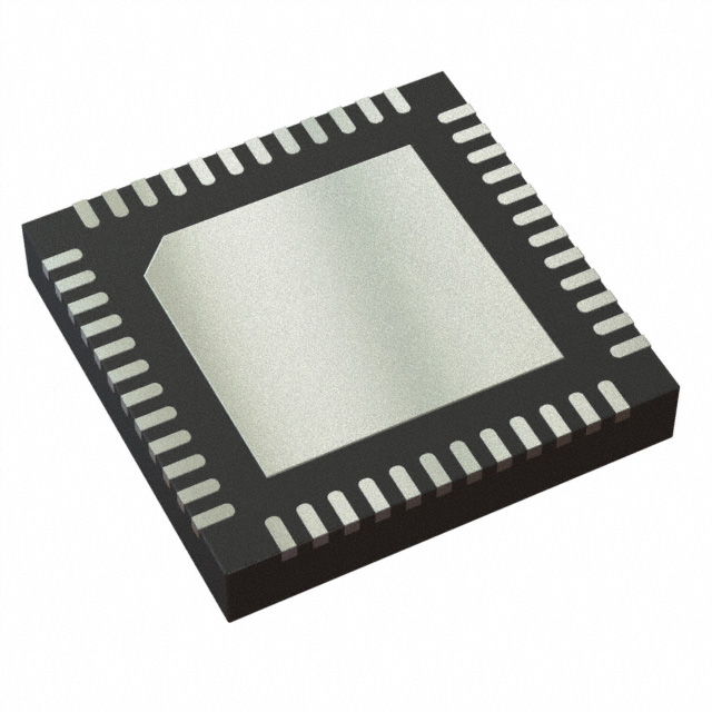
The Texas Instruments TPS65218B1RSLR is an integrated power management circuit designed for ARM Cortex-A8/A9 SoCs and FPGAs. This PMIC offers a versatile solution with multiple output converters, including three adjustable step-down converters (DCDC1, DCDC2, DCDC3) and one adjustable buck-boost converter (DCDC4).
DCDC1, DCDC2, and DCDC3 converters have a default output voltage of 1.1V, 1.1V, and 1.2V respectively, each capable of up to 1.8A. Their output voltages are adjustable from 0.85V to 1.675V (DCDC1/DCDC2) and 0.9V to 3.4V (DCDC3). The DCDC4 converter defaults to 3.3V with a maximum output current of 1.6A. The device operates with an input voltage range from 2.2V to 5.5V.
This PMIC is housed in a 48-VQFN (6x6) package and is designed for surface mounting. It operates within an ambient temperature range of -40°C to 105°C. The TPS65218B1RSLR features include power-save mode at light load and 100% duty cycle for lowest dropout.
This product is not recommended for new designs. It continues to be available for existing customers, but new designs should consider an alternate product.
| Qty | Low | High |
|---|---|---|
| 1+ | $3.81 | $3.81 |
Estimated market price range - modelled values for guidance only, not live distributor offers.
The input voltage range is from 2.2 V to 5.5 V.
The output voltage range is from 0.8 V to 3.5 V.
The maximum output current is 1.8 A.
The operating temperature range is -40°C to 105°C.
It is available in a 48-VQFN (6x6) package and a 48-VFQFN Exposed Pad package.
It is designed for ARM® Cortex™ -A8/A9 SOCs and FPGAs.
No, this product is not recommended for new designs. It is available for existing customers, but new designs should consider an alternate product.