

| Distributor | Stock | Pricing | MOQ | PKG | Lead Time | Date Code | On Order Quantity | On Order Delivery | |
|---|---|---|---|---|---|---|---|---|---|
|
515 pcs
|
515 pcs | On Request | 1 | On Request | On Request | 25+ | On Request | On Request |
| Category | |
| Manufacturer Name | |
| Current | |
| Frequency | |
| Function | |
| Mounting Type | |
| Number of Outputs | |
| Operating Temperature | |
| Output Configuration | |
| Output Type | |
| Quiescent Current | |
| SVHC Present | |
| Supplier Device Package | |
| Synchronous Rectifier | |
| Tape & Reel | |
| Topology | |
| Voltage |
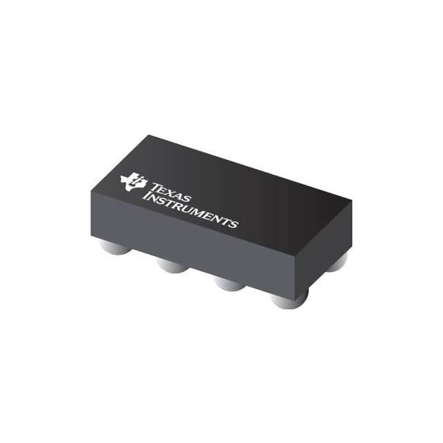
The TPS631010YBGR from Texas Instruments is a constant frequency, peak current mode control buck-boost converter. It is housed in a tiny wafer chip scale package (WCSP) and offers a 3A peak switch current limit. The device supports an input voltage range of 1.6V to 5.5V and an adjustable output voltage range of 1.2V to 5.5V.
This converter architecture allows for seamless transitions between boost, buck, and 3-cycle buck-boost modes depending on the input voltage relative to the output voltage. It features a low quiescent current of 8μA typical, enabling high efficiency at light load conditions through automatic power save mode. The fixed switching frequency is 2MHz.
Key features include overcurrent protection, short-circuit protection, integrated soft start, overtemperature protection, and overvoltage protection. The small solution size is further enhanced by the requirement for a small 1-μH inductor. The WCSP package measures 1.803mm x 0.905mm.
Applications for the TPS631010YBGR include TWS devices, system pre-regulators for smartphones and tablets, point-of-load regulation for sensors and adapters, and voltage stabilizers for datacom and optical modules.
| Qty | Low | High |
|---|---|---|
| 1+ | $0.60 | $0.60 |
Estimated market price range - modelled values for guidance only, not live distributor offers.
The input voltage range is 1.6V to 5.5V.
The output voltage is adjustable from 1.2V to 5.5V.
The device can provide 2A output current for VIN ≥ 3V, VOUT = 3.3V, and 1.5A output current for VIN ≥ 2.7V, VOUT = 3.3V.
The switching frequency is fixed at 2MHz.
The operating temperature range is -40°C to 125°C (TJ).
It is supplied in an 8-DSBGA (WCSP) package with dimensions of 1.803mm x 0.905mm.