

| Distributor | Stock | Pricing | MOQ | PKG | Lead Time | Date Code | On Order Quantity | On Order Delivery | |
|---|---|---|---|---|---|---|---|---|---|
|
81,000 pcs
|
81000 pcs | On Request | 1 | On Request | On Request | 21+ | On Request | On Request | |
|
1,086 pcs
|
1086 pcs | On Request | 1 | On Request | On Request | On Request | On Request | On Request | |
|
217 pcs
|
217 pcs | On Request | 1 | On Request | On Request | 15+ | On Request | On Request |
| Category | |
| Manufacturer Name | |
| Current | |
| Duty Cycle | |
| Frequency | |
| Function | |
| Mounting Type | |
| Number of Outputs | |
| Operating Temperature | |
| Output Configuration | |
| Output Type | |
| Output Voltage | |
| Quiescent Current | |
| Supplier Device Package | |
| Supplier Package | |
| Synchronous Rectifier | |
| Topology | |
| Voltage |
The Texas Instruments TPS63036YFGR is an active DC DC switching regulator designed for high-efficiency operation. This buck-boost converter utilizes a single inductor and supports an input voltage range of 1.8 V to 5.5 V, with a requirement of over 2 V for device start-up. The output voltage is adjustable from 1.2 V to 5.5 V.
Key electrical characteristics include a switch current limit of 1 A (typical) and a fixed switching frequency of 2.4 MHz. The device operates with a low quiescent current of 25 µA, featuring a power-save mode with seamless transition. It also supports frequency synchronization to an external clock.
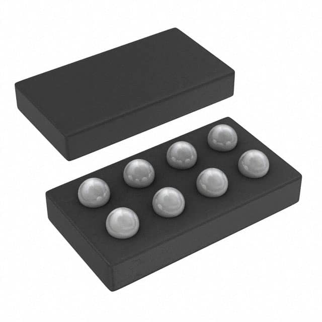
Packaged in a tiny 8-pin wafer chip scale package (WCSP), measuring 1.814 mm x 1.076 mm, the TPS63036YFGR is suitable for space-constrained applications. The operating temperature range is -40°C to 125°C. Safety features include overtemperature and overvoltage protection, along with load disconnect during shutdown.
| Qty | Low | High |
|---|---|---|
| 1+ | $0.87 | $0.87 |
Estimated market price range - modelled values for guidance only, not live distributor offers.
The input voltage range is 1.8 V to 5.5 V, with a requirement of over 2 V for device start-up.
The output voltage is adjustable from 1.2 V to 5.5 V.
The switch current limit is typically 1 A.
The operating quiescent current is typically 25 µA.
The device operates at a fixed switching frequency of 2.4 MHz.
The operating temperature range is -40°C to 125°C.
It is supplied in a tiny 8-pin wafer chip scale package (WCSP), also referred to as 8-DSBGA.