

| Distributor | Stock | Pricing | MOQ | PKG | Lead Time | Date Code | On Order Quantity | On Order Delivery | |
|---|---|---|---|---|---|---|---|---|---|
|
146,000 pcs
|
146000 pcs | On Request | 1 | On Request | On Request | On Request | On Request | On Request | |
|
15,000 pcs
|
15000 pcs | On Request | 1 | On Request | On Request | 21+ | On Request | On Request | |
|
3,101 pcs
|
3101 pcs | On Request | 1 | On Request | On Request | On Request | On Request | On Request | |
|
2,658 pcs
|
2658 pcs | On Request | 1 | On Request | On Request | 21+ | On Request | On Request | |
|
500 pcs
|
500 pcs | On Request | 1 | On Request | On Request | On Request | On Request | On Request | |
|
1 pcs
|
1 pcs | On Request | 1 | On Request | On Request | On Request | On Request | On Request |
| Category | |
| Manufacturer Name | |
| Current | |
| Duty Cycle | |
| Function | |
| Input Voltage | |
| Mounting Type | |
| Number of Outputs | |
| Operating Temperature | |
| Output Configuration | |
| Output Type | |
| Output Voltage | |
| Supplier Device Package | |
| Synchronous Rectifier | |
| Topology | |
| Voltage |
The TPS61291DRVR from Texas Instruments is a DC/DC switching regulator designed for step-up (boost) conversion. It operates with an input voltage range of 0.9V to 5V and provides a programmable output voltage between 2.5V and 3.3V. The device has a typical switch current limit of 1A and a quiescent current of 15nA in bypass mode and 5.7µA in boost mode.
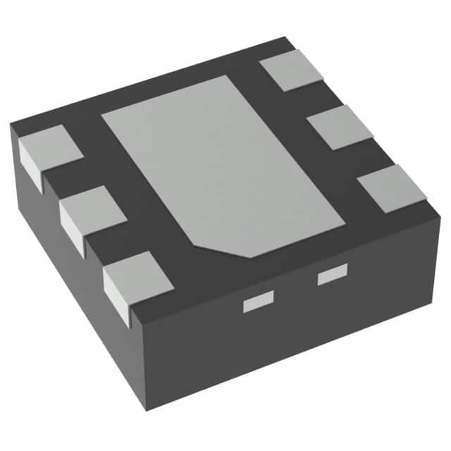
This regulator features synchronous rectification and a pass-through mode, allowing for efficient power management. It is housed in a 6-WSON (2x2) package, suitable for surface mount applications. The operating temperature range is specified from -40°C to 125°C, making it suitable for various environmental conditions.
| Qty | Low | High |
|---|---|---|
| 1+ | $0.62 | $0.62 |
Estimated market price range - modelled values for guidance only, not live distributor offers.
The input voltage range is 0.9V to 5V.
The output voltage is programmable from 2.5V to 3.3V.
The typical switch current limit is 1A, and the switch current is 700mA.
The operating temperature range is -40°C to 125°C.
It is available in a 6-WDFN exposed pad package, also referred to as 6-WSON (2x2).
Yes, it has a synchronous rectifier.
The quiescent current is 15nA in bypass mode and 5.7µA in boost mode.