

| Distributor | Stock | Pricing | MOQ | PKG | Lead Time | Date Code | On Order Quantity | On Order Delivery | |
|---|---|---|---|---|---|---|---|---|---|
|
39,000 pcs
|
39000 pcs | On Request | 1 | On Request | On Request | 18PB | On Request | On Request |
| Category | |
| Manufacturer Name | |
| Current | |
| Efficiency | |
| Frequency | |
| Function | |
| Input Voltage | |
| Mounting Type | |
| Number of Outputs | |
| Operating Temperature | |
| Output Configuration | |
| Output Type | |
| Output Voltage | |
| Supplier Device Package | |
| Synchronous Rectifier | |
| Topology | |
| Voltage |
The Texas Instruments TPS61259YFFR is a high-efficiency step-up (boost) converter designed for low-power, battery-powered portable applications. It operates with an input voltage range from 2.3 V to 5.5 V and provides a fixed output voltage of 5.1 V with a maximum output current of 3.9 A (switch). The device boasts 93% efficiency at 3.5 MHz operation and features low quiescent currents of 21 µA in standby mode and 37 µA in normal operation.
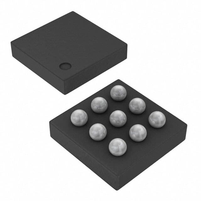
This boost converter requires only three surface-mount external components, contributing to a total solution size of less than 25 mm². It is housed in a compact 9-pin NanoFree™ (CSP) package, specifically a 9-DSBGA, suitable for space-constrained designs. The TPS61259YFFR includes thermal shutdown and overload protection, along with selectable standby or true load disconnect during shutdown, enhancing its reliability and power management capabilities.
Key electrical characteristics include a wide input voltage range, ±2% total DC voltage accuracy, and a light-load PFM mode. The device is suitable for applications requiring efficient power conversion from a discharging battery. Its surface-mount package and minimal external component count make it an attractive choice for portable electronics, wearables, and other compact devices.
| Qty | Low | High |
|---|---|---|
| 1+ | $0.42 | $0.42 |
Estimated market price range - modelled values for guidance only, not live distributor offers.
The input voltage range for the TPS61259YFFR is 2.3 V to 5.5 V.
The output voltage of the TPS61259YFFR is 5.1 V.
The TPS61259YFFR has a maximum efficiency of 93% during 3.5-MHz operation.
The quiescent current in standby mode for the TPS61259YFFR is 21 µA.
The TPS61259YFFR operates within a temperature range of -40°C to 125°C.
The TPS61259YFFR comes in a 9-DSBGA package, also known as 9-UFBGA, DSBGA.
The TPS61259YFFR is designed for Surface Mount applications.