

| Distributor | Stock | Pricing | MOQ | PKG | Lead Time | Date Code | On Order Quantity | On Order Delivery | |
|---|---|---|---|---|---|---|---|---|---|
|
7,800 pcs
|
7800 pcs | On Request | 1 | On Request | On Request | 16+ | On Request | On Request | |
|
3,600 pcs
|
3600 pcs | On Request | 1 | On Request | On Request | On Request | On Request | On Request | |
|
1,846 pcs
|
1846 pcs | On Request | 1 | On Request | On Request | 0814+ | On Request | On Request |
| Category | |
| Manufacturer Name | |
| Channel Type | |
| Driven Configuration | |
| Gate Type | |
| High Side Voltage | |
| Input Type | |
| Mounting Type | |
| Number of Drivers | |
| Operating Temperature | |
| Propagation Delay | |
| Quiescent Current | |
| Rise | |
| Supplier Device Package | |
| Supplier Package | |
| Voltage |
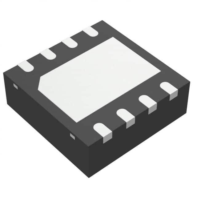
The Texas Instruments TPS28226DRBR is a high-speed driver for N-channel complimentary driven power MOSFETs, featuring adaptive dead-time control. This driver is optimized for use in a variety of high-current one and multi-phase DC-to-DC converters, providing high efficiency, small size, and low EMI emissions.
Key electrical specifications include a wide gate drive voltage range of 4.5 V to 8.8 V, with best efficiency at 7 V to 8 V. The power system train input voltage ranges from 3 V to 27 V, and it accepts wide input PWM signals from 2.0 V to 13.2 V amplitude. It offers a high frequency operation with a 14-ns propagation delay and 10-ns rise/fall times, allowing for FSW up to 2 MHz. The device is capable of driving MOSFETs with >=40-A current per phase and features a low-side driver sink on-resistance of 0.4 Ω to prevent shoot-through current.
Applications for the TPS28226DRBR include multi-phase DC-to-DC converters, desktop and server VRMs, portable and notebook regulators, and synchronous rectification for isolated power supplies. The device is available in an economical 8-SON (3x3 mm) package, suitable for space-saving designs.
Additional features include 3-state PWM input for power stage shutdown, space-saving Enable (Input) and Power Good (Output) signals on the same pin, thermal shutdown, and UVLO protection. The internal bootstrap diode allows for N-channel MOSFETs in a half-bridge configuration.
| Qty | Low | High |
|---|---|---|
| 1+ | $0.61 | $0.61 |
Estimated market price range - modelled values for guidance only, not live distributor offers.
The input supply voltage range is 3 V to 27 V for the system power train, with a gate drive supply of 4.5 V to 8.8 V.
8-VDFN Exposed Pad package, also referred to as 8-SON (3x3 mm).
-40°C to 125°C.
4 A peak sink current and 2 A peak source current.
14 ns typical propagation delay.
33 V.
0.35 mA.