

| Distributor | Stock | Pricing | MOQ | PKG | Lead Time | Date Code | On Order Quantity | On Order Delivery | |
|---|---|---|---|---|---|---|---|---|---|
|
100,000 pcs
|
100000 pcs | On Request | 1 | On Request | On Request | On Request | On Request | On Request | |
|
246 pcs
|
246 pcs | On Request | 1 | On Request | On Request | 13+ | On Request | On Request | |
|
26 pcs
|
26 pcs | On Request | 1 | On Request | On Request | On Request | On Request | On Request |
| Category | |
| Manufacturer Name | |
| Channel Type | |
| Driven Configuration | |
| Features | |
| Gate Type | |
| High Side Voltage | |
| Input Type | |
| Mounting Type | |
| Number of Drivers | |
| Operating Temperature | |
| Quiescent Current | |
| Rise | |
| Supplier Device Package | |
| Supplier Package | |
| Tape & Reel | |
| Voltage |
The Texas Instruments TPS28225DRBT is a high-frequency half-bridge gate driver with a 4-A peak output current and a 27-V system voltage capability. It is designed to drive two N-channel MOSFETs with adaptive dead time control, featuring 14ns propagation delay and 10ns rise/fall times, enabling switching frequencies up to 2MHz.
This gate driver operates with a wide gate drive voltage range from 4.5V to 8.8V and a power system train input voltage from 3V to 27V. It accepts input PWM signals with amplitudes from 2.0V to 13.2V and can drive MOSFETs with currents of 40A per phase. The device includes undervoltage lockout (UVLO) protection, thermal shutdown, and an internal bootstrap diode.
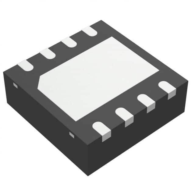
Available in an 8-VSON (3x3 mm) package, the TPS28225DRBT is suitable for surface mount applications. Its low-side driver sink on-resistance of 0.4Ω helps prevent shoot-through current. The driver configuration is single, supporting synchronous rectification and PWM input.
Key electrical specifications include a maximum bootstrap supply voltage of 33V, a minimum input supply voltage of 4.5V, and a maximum input supply voltage of 8V. The quiescent current is 0.35mA. Input logic is TTL compatible.
| Qty | Low | High |
|---|---|---|
| 1+ | $1.03 | $1.03 |
Estimated market price range - modelled values for guidance only, not live distributor offers.
The peak output current is 4 A.
The operating temperature range is -40°C to 125°C.
The undervoltage lockout typical voltage is 3.5 V.
The propagation delay time is 0.014 µs.
The rise time is 10 ns and the fall time is 5 ns.
The quiescent current is 0.35 mA.
The device allows switching frequencies up to 2 MHz.