

| Distributor | Stock | Pricing | MOQ | PKG | Lead Time | Date Code | On Order Quantity | On Order Delivery | |
|---|---|---|---|---|---|---|---|---|---|
|
16,360 pcs
|
16360 pcs | On Request | 1 | On Request | On Request | On Request | On Request | On Request | |
|
9,388 pcs
|
9388 pcs | On Request | 1 | On Request | On Request | On Request | On Request | On Request | |
|
9,353 pcs
|
9353 pcs | On Request | 1 | On Request | On Request | On Request | On Request | On Request | |
|
7,000 pcs
|
7000 pcs | On Request | 1 | On Request | On Request | 0842+ | On Request | On Request | |
|
286 pcs
|
286 pcs | On Request | 1 | On Request | On Request | 12+ | On Request | On Request |
| Category | |
| Manufacturer Name | |
| Channel Type | |
| Current | |
| Driven Configuration | |
| Gate Type | |
| High Side Voltage | |
| Input Type | |
| Mounting Type | |
| Number of Drivers | |
| Operating Temperature | |
| Quiescent Current | |
| Rise | |
| Supplier Device Package | |
| Supplier Package | |
| Voltage |
The Texas Instruments TPS28225DRBR is an active half-bridge gate driver IC. It is designed to drive two N-channel MOSFETs with adaptive dead time control, featuring 14ns adaptive dead time.
This device supports a wide gate drive voltage range from 4.5V to 8.8V, with optimal efficiency typically seen between 7V and 8V. The power system train input voltage can range from 3V up to 27V, and it accepts input PWM signals from 2.0V to 13.2V amplitude. It is capable of driving MOSFETs with currents of 40A per phase.
Key electrical specifications include a peak output current of 4A, a propagation delay time of 14ns, and rise/fall times of 10ns and 5ns respectively. The operating temperature range is -40°C to 125°C. It features undervoltage lockout (UVLO) typically at 3.5V and a low-side driver sink on-resistance of 0.4Ω to prevent shoot-through current.
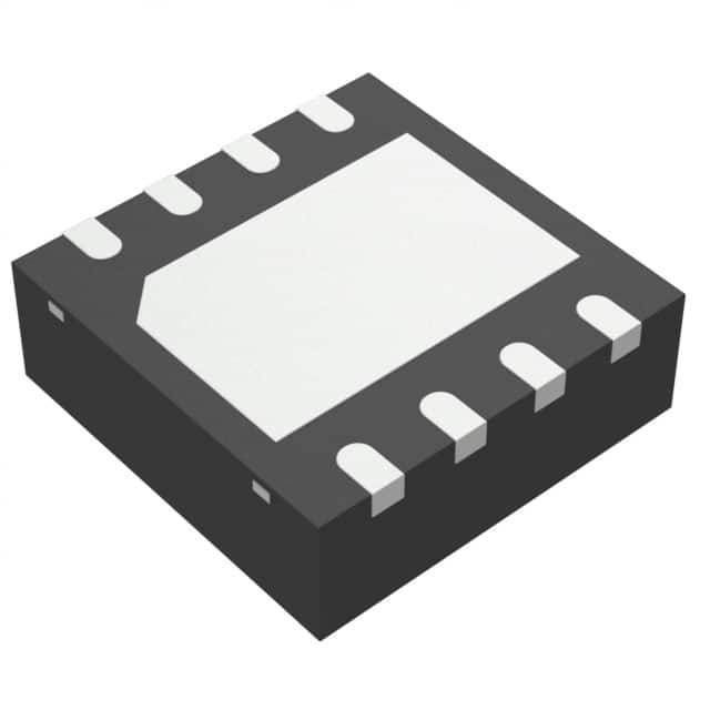
The TPS28225DRBR is available in an 8-SON (3x3mm) package, offering a space-saving solution. It includes features like a 3-state PWM input for power stage shutdown, an enable input, and a power good output signal on the same pin. Thermal shutdown and an internal bootstrap diode are also integrated.
| Qty | Low | High |
|---|---|---|
| 1+ | $0.70 | $0.70 |
Estimated market price range - modelled values for guidance only, not live distributor offers.
The input supply voltage range is 4.5V to 8V, the gate drive voltage is 4.5V to 8.8V, and the power system train input is 3V to 27V.
It is available in an 8-VDFN Exposed Pad package, also referred to as 8-SON (3x3).
The junction temperature operating range is -40°C to 125°C.
4A.
Up to 2 MHz.
14 ns typical.