

| Distributor | Stock | Pricing | MOQ | PKG | Lead Time | Date Code | On Order Quantity | On Order Delivery | |
|---|---|---|---|---|---|---|---|---|---|
|
3,173 pcs
|
3173 pcs | On Request | 1 | On Request | On Request | 22+ | On Request | On Request | |
|
24 pcs
|
24 pcs | On Request | 1 | On Request | On Request | On Request | On Request | On Request |
| Category | |
| Manufacturer Name | |
| Current | |
| Features | |
| Input Type | |
| Interface | |
| Mounting Type | |
| Number of Outputs | |
| Operating Temperature | |
| Output Configuration | |
| Output Type | |
| Quiescent Current | |
| Ratio | |
| Rds On (Typ) | |
| SVHC Present | |
| Supplier Device Package | |
| Switch Type | |
| Voltage |
The TPS22965DSGT from Texas Instruments is a single-channel load switch IC. It operates with an input voltage range from 0.8 V to 5.7 V and can handle a maximum continuous current of 6 A. The device features a low on-resistance of 16 mΩ at typical operating conditions, minimizing power loss.
Designed for flexibility, the TPS22965DSGT includes features such as configurable rise time to manage inrush current and an optional output discharge function. Its low quiescent current of 50 µA makes it suitable for power-sensitive applications. The control input threshold is low, enabling direct interfacing with 1.2-V, 1.8-V, 2.5-V, and 3.3-V logic.
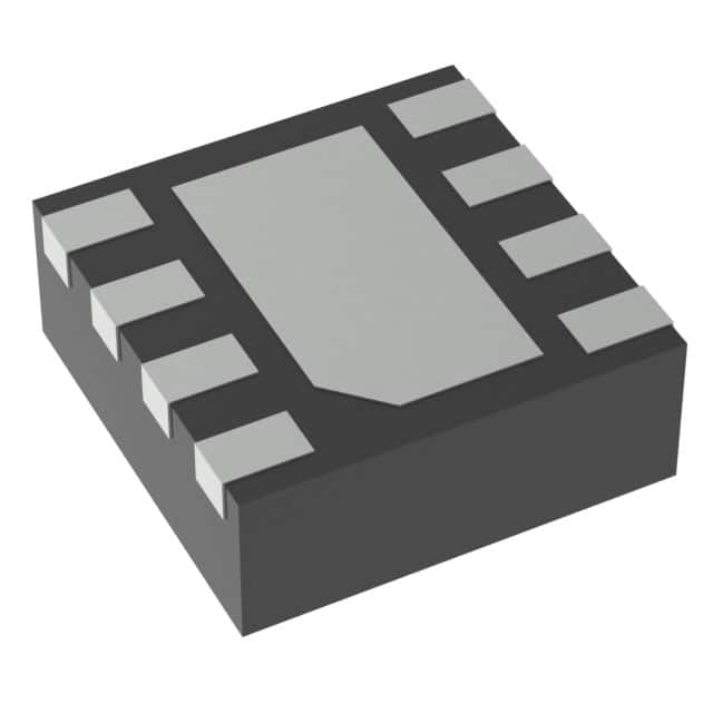
This load switch is available in an 8-WSON (2x2) package with an exposed thermal pad for improved heat dissipation. It is designed for surface mount applications and operates within an ambient temperature range of -40°C to 105°C. The TPS22965DSGT is suitable for various power distribution and load switching tasks in electronic systems.
| Qty | Low | High |
|---|---|---|
| 1+ | $0.53 | $0.53 |
Estimated market price range - modelled values for guidance only, not live distributor offers.
The input voltage range is 0.8 V to 5.7 V.
It is available in 8-WSON (2x2) and 8-WFDFN Exposed Pad packages.
The operating temperature range is -40°C to 105°C.
The maximum continuous switch current is 6 A.
The typical on-resistance is 16 mΩ under various bias conditions (VIN=5V, 3.6V, or 1.8V with VBIAS=5V).
The low quiescent current is 50 µA.
It is a high-side, N-channel output with 1:1 ratio and non-inverting input.