

| Distributor | Stock | Pricing | MOQ | PKG | Lead Time | Date Code | On Order Quantity | On Order Delivery | |
|---|---|---|---|---|---|---|---|---|---|
|
9,043 pcs
|
9043 pcs | On Request | 1 | On Request | On Request | 1751+ | On Request | On Request |
| Category | |
| Manufacturer Name | |
| Current | |
| Fault Protection | |
| Features | |
| Input Type | |
| Interface | |
| Mounting Type | |
| Number of Outputs | |
| Operating Temperature | |
| Output Configuration | |
| Output Type | |
| Quiescent Current | |
| Ratio | |
| Rds On (Typ) | |
| Supplier Device Package | |
| Supplier Package | |
| Switch Type | |
| Voltage |
The Texas Instruments TPS22925CNYPHR is an active load switch IC designed for efficient power management. It supports an input voltage range from 0.65V to 3.6V and can handle a maximum continuous switch current of 3A. The device boasts a low typical on-resistance of 9.2mΩ at 3.6V input, minimizing voltage drop and power loss.
Key features include inrush current control, quick output discharge (QOD), reverse current blocking, and reverse current protection, enhancing system reliability. The TPS22925CNYPHR offers a slew rate controlled output, with typical rise times of 97µs for TPS22925Bx variants and 810µs for TPS22925Cx variants at 3.6V input. It operates within a temperature range of -40°C to 105°C.
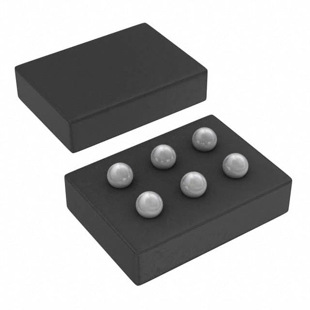
This load switch is housed in a compact 6-DSBGA package, suitable for surface mount applications where space is constrained. The interface is a simple On/Off control, compatible with 1.5V, 1.8V, 2.5V, or 3.3V logic levels. Its general-purpose switch type and high-side output configuration make it versatile for various power switching needs.
| Qty | Low | High |
|---|---|---|
| 1+ | $0.18 | $0.18 |
Estimated market price range - modelled values for guidance only, not live distributor offers.
The input voltage range is 0.65 V to 3.6 V.
The maximum continuous switch current is 3 A.
The typical on-resistance is 9.2 mΩ at V_IN = 3.6 V.
The operating temperature range is -40°C to 105°C.
The device is offered in a 6-XFBGA, DSBGA package (6-DSBGA).
Yes, it includes reverse current protection and reverse current blocking when disabled.
The typical rise time is 810 µs at V_IN = 3.6 V.