

| Distributor | Stock | Pricing | MOQ | PKG | Lead Time | Date Code | On Order Quantity | On Order Delivery | |
|---|---|---|---|---|---|---|---|---|---|
|
1,487 pcs
|
1487 pcs | On Request | 1 | On Request | On Request | On Request | On Request | On Request | |
|
205 pcs
|
205 pcs | On Request | 1 | On Request | On Request | On Request | On Request | On Request | |
|
187 pcs
|
187 pcs | On Request | 1 | On Request | On Request | 1744 | On Request | On Request |
| Category | |
| Manufacturer Name | |
| Applications | |
| Current | |
| Delay Time | |
| FET Type | |
| Internal Switch(s) | |
| Mounting Type | |
| Operating Temperature | |
| Quiescent Current | |
| Ratio | |
| Supplier Device Package | |
| Supplier Package | |
| Type | |
| Voltage |
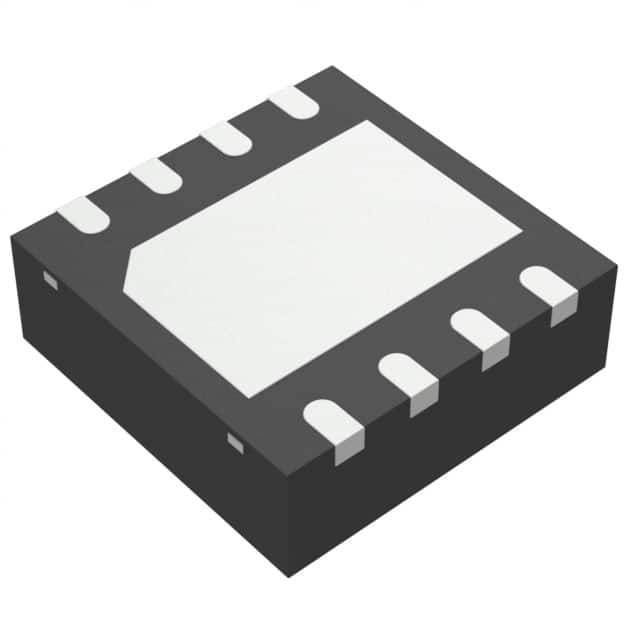
The Texas Instruments TPS2113ADRBR is an active power multiplexer designed for source selection in power management applications. It features two inputs (IN1, IN2) and one output, with a wide operating voltage range from 2.8V to 5.5V.
Key electrical specifications include a typical RDS(on) of 84 mΩ for both input channels, enabling efficient power transfer. The device can handle an output current of up to 1.25A. It also offers a low quiescent current of 0.5 µA, making it suitable for low-power applications.
This power mux includes features such as adjustable current limit, inrush current control, reverse current blocking, thermal shutdown, and under-voltage lockout. It provides a power good signal and supports auto-switching operating modes. The TPS2113ADRBR is available in an 8-SON (3x3 mm) package, suitable for surface mounting.
Designed for applications like handheld and mobile devices, the TPS2113ADRBR simplifies power source management by automatically selecting the optimal input or providing a status signal. Its compact package and integrated features make it a versatile solution for space-constrained designs.
| Qty | Low | High |
|---|---|---|
| 1+ | $0.95 | $0.95 |
Estimated market price range - modelled values for guidance only, not live distributor offers.
The input voltage range is 2.8V to 5.5V.
The maximum output current is 2A per channel.
It comes in an 8-VDFN exposed pad package (8-SON 3x3mm).
The typical quiescent current is 0.5 µA.
The typical RDS(on) is 84 mΩ for both input channels.
The operating temperature range is -40°C to 85°C.
The delay time is 1 ms.