

| Distributor | Stock | Pricing | MOQ | PKG | Lead Time | Date Code | On Order Quantity | On Order Delivery | |
|---|---|---|---|---|---|---|---|---|---|
|
141 pcs
|
141 pcs | On Request | 1 | On Request | On Request | 05+ | On Request | On Request |
| Category | |
| Manufacturer Name | |
| Current | |
| Drain to Source Voltage (Vdss) | |
| Drive Voltage (Max Rds On, Min Rds On) | |
| FET Type | |
| Gate Charge (Qg) (Max) @ Vgs | |
| Mounting Type | |
| Operating Temperature | |
| Power Dissipation (Max) | |
| Rds On (Max) @ Id, Vgs | |
| Supplier Device Package | |
| Supplier Package | |
| Technology | |
| Vgs (Max) | |
| Vgs(th) (Max) @ Id |
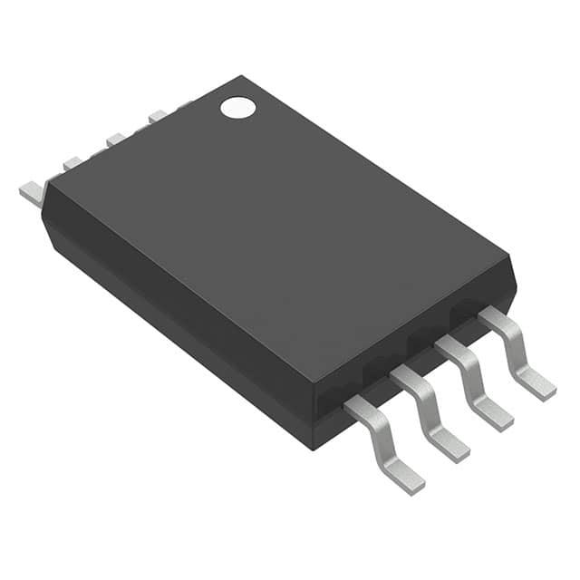
The Texas Instruments TPS1100PWR is a single P-channel enhancement-mode MOSFET optimized for 3-V or 5-V power distribution in battery-powered systems. It operates with a drain-to-source voltage (Vdss) of 15V and can handle a continuous drain current of 1.27A at ambient temperature. The MOSFET exhibits a low on-resistance (Rds On) of 180mOhm at a gate-to-source voltage (Vgs) of 10V and a drain current (Id) of 1.5A. Its gate threshold voltage (Vgs(th)) is a maximum of 1.5V at 250µA. The device is designed with a maximum gate-to-source voltage of +2V and -15V.
This MOSFET is available in an 8-TSSOP package, measuring 0.173 inches (4.40mm) in width, suitable for surface mount applications. It has a maximum power dissipation of 504mW at ambient temperature and an operating temperature range of -40°C to 150°C (TJ). The TPS1100PWR is designed for low-voltage switching applications, such as power switches for pulse-width-modulated (PWM) controllers or motor/bridge drivers, where maximizing battery life is a primary concern due to its low quiescent current.
The TPS1100PWR is RoHS3 compliant and has an MSL rating of 1 (Unlimited). Its REACH status is unaffected. The device is manufactured using Texas Instruments' LinBiCMOS process.
| Qty | Low | High |
|---|---|---|
| 1+ | $0.73 | $0.73 |
Estimated market price range - modelled values for guidance only, not live distributor offers.
The maximum drain-to-source voltage is 15V.
It is a P-Channel MOSFET.
The component uses an 8-TSSOP surface mount package.
The maximum continuous drain current is 1.27A at ambient temperature.
The operating junction temperature range is -40°C to 150°C.
The maximum on-resistance is 180mΩ when tested at 1.5A and 10V.