
BC847B/215
Nexperia USA Inc.
The Nexperia USA Inc. BC847B/215 is a bipolar transistor. It is RoHS3 Compliant and has an MSL Level 1 rating.


| Distributor | Stock | Pricing | MOQ | PKG | Lead Time | Date Code | On Order Quantity | On Order Delivery | |
|---|---|---|---|---|---|---|---|---|---|
|
120,533 pcs
|
120533 pcs | On Request | 1 | On Request | On Request | On Request | On Request | On Request | |
|
1,100 pcs
|
1100 pcs | On Request | 1 | On Request | On Request | On Request | On Request | On Request |
| Category | |
| Manufacturer Name | |
| SVHC Present |
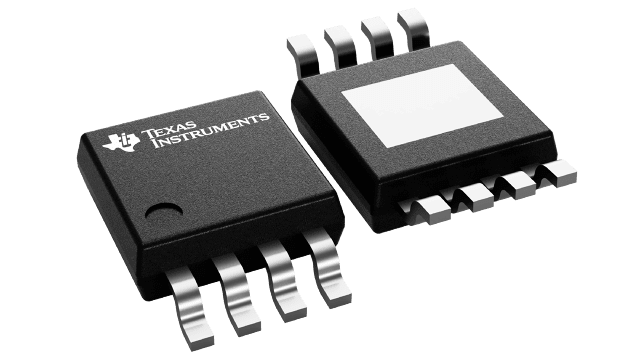
The TLV4112IDGN is a dual-channel CMOS operational amplifier from Texas Instruments. It features a gain bandwidth product of 2.7 MHz and a typical slew rate of 1.57 V/µs. The device operates from a supply voltage range of 2.5 V to 6 V and can deliver a typical output current of 0.32 A. It has a rail-to-rail output stage and a CMOS architecture.
The amplifier offers a maximum input offset voltage of 3.5 mV with a typical offset drift of 3 µV/°C. The typical quiescent current per channel is 0.7 mA. It provides a common-mode rejection ratio of 68 dB and a maximum input bias current of 25 pA. The operating temperature range is -40°C to 125°C.
The TLV4112IDGN is available in an HVSSOP (DGN) package with a footprint of 14.7 mm² (3 mm × 4.9 mm). This package is suitable for space-constrained applications requiring high output drive capability.
| Qty | Low | High |
|---|---|---|
| 1+ | $1.89 | $1.89 |
Estimated market price range - modelled values for guidance only, not live distributor offers.
The supply voltage range is 2.5 V to 6 V.
The typical gain bandwidth product is 2.7 MHz.
The operating temperature range is -40°C to 125°C.
The TLV4112IDGN is available in an HVSSOP (DGN) package.
The typical output current is 0.32 A.
Yes, it has rail-to-rail output.