

| Distributor | Stock | Pricing | MOQ | PKG | Lead Time | Date Code | On Order Quantity | On Order Delivery | |
|---|---|---|---|---|---|---|---|---|---|
|
321,204 pcs
|
321204 pcs | On Request | 1 | On Request | On Request | On Request | On Request | On Request | |
|
1,800 pcs
|
1800 pcs | On Request | 1 | On Request | On Request | On Request | On Request | On Request |
| Category | |
| Manufacturer Name | |
| Current | |
| Current Drain (Id) | |
| Drain to Source Voltage (Vdss) | |
| FET Type | |
| Halogen Free | |
| Input Capacitance | |
| Input Capacitance (Ciss) (Max) @ Vds | |
| Mounting Type | |
| Operating Temperature | |
| Power | |
| SVHC Present | |
| Storage Temperature | |
| Supplier Device Package | |
| Tape & Reel | |
| Voltage |
The TF412ST5G from On Semiconductor is an N-Channel Junction Field-Effect Transistor (JFET) designed for low-frequency general-purpose amplification, impedance conversion, and infrared sensor applications.
This device features a maximum drain-to-source voltage (VDSX) of 30V and a maximum gate current (IG) of 10mA. The drain current (IDSS) ranges from 1.2mA to 3.0mA at 10V drain-to-source voltage and 0V gate-to-source voltage. Its forward transfer admittance (|yfs|) is typically between 3.0mS and 5.0mS at 1kHz.
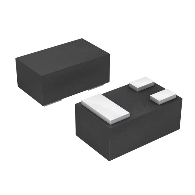
The JFET operates within a junction temperature range of -55°C to +150°C and has a maximum power dissipation of 100mW. It is supplied in an ultrasmall SOT-883 (XDFN3) surface-mount package, facilitating miniaturization in end products.
The TF412ST5G is a Pb-Free and Halogen Free device, making it suitable for environmentally conscious designs.
| Qty | Low | High |
|---|---|---|
| 1+ | $0.99 | $0.99 |
Estimated market price range - modelled values for guidance only, not live distributor offers.
30 V.
10 mA.
100 mW.
150°C.
3-XFDFN, also known as SOT-883 (XDFN3) with dimensions 1x0.6mm.
-0.18 to -1.5 V.
4 pF typical.