

| Distributor | Stock | Pricing | MOQ | PKG | Lead Time | Date Code | On Order Quantity | On Order Delivery | |
|---|---|---|---|---|---|---|---|---|---|
|
500 pcs
|
500 pcs | On Request | 1 | On Request | On Request | On Request | On Request | On Request |
| Category | |
| Manufacturer Name | |
| Applications | |
| Current | |
| Mounting Type | |
| Operating Temperature | |
| Operating Voltage | |
| Quiescent Current | |
| Supplier Device Package | |
| Voltage |
The TDA3681TH/N2S,518 from NXP Semiconductors is a specialized integrated circuit designed for power management applications. This device functions as a multiple voltage regulator, incorporating a power switch and an ignition buffer.
Key electrical specifications include a supply voltage range of 9.5V to 18V, with an extended range noted in the datasheet from -18V to 50V. It operates with a quiescent current of 110µA. The device is designed to function within an operating temperature range of -40°C to 85°C.
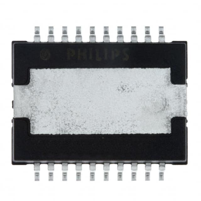
Packaged in a 20-HSOP and also specified as a 20-SOIC (0.433", 11.00mm Width) Exposed Pad, this component is suitable for surface mount applications. Its features include low noise behavior, stability with small output capacitors, and various protection mechanisms such as reverse polarity safety, thermal protection, and foldback current limiting.
The TDA3681 is intended for use in automotive applications, such as car radios, where a microcontroller may or may not be present. It offers multiple regulators, a power switch, reset and hold outputs, and an independent ignition buffer.
| Qty | Low | High |
|---|---|---|
| 1+ | $0.75 | $0.75 |
Estimated market price range - modelled values for guidance only, not live distributor offers.
The operating voltage range is 9.5V to 18V.
The operating temperature range is -40°C to 85°C.
It is supplied in a 20-HSOP package, also described as 20-SOIC (0.433", 11.00mm Width) Exposed Pad.
This component is designed for surface mount.
The quiescent current is 110µA.
According to the datasheet, the supply voltage range is from -18 V to 50 V.