Ready to onboard?
Are you ready to join DistyParts and
grow your business?


| Distributor | Stock | Pricing | MOQ | PKG | Lead Time | Date Code | On Order Quantity | On Order Delivery | |
|---|---|---|---|---|---|---|---|---|---|
|
33,020 pcs
|
33020 pcs | On Request | 1 | On Request | On Request | On Request | On Request | On Request |
| Category | |
| Manufacturer Name | |
| Applications | |
| Automotive Grade | |
| Breakdown Voltage (Minimum/Typical/Maximum @ IT = 1 mA, I/O Pin to GND) | |
| Capacitance | |
| Capacitance (Maximum @ I/O to GND) | |
| Capacitance @ Frequency | |
| Current | |
| ESD Protection (Maximum @ IEC 61000-4-2 Air) | |
| ESD Protection (Maximum @ IEC 61000-4-2 Contact) | |
| ESD Protection (Maximum @ ISO 10605 330 pF / 2 kΩ Contact) | |
| Halogen Free | |
| Lead Solder Temperature | |
| Mounting Type | |
| Operating Temperature | |
| Pb-Free | |
| Peak Pulse Current (Maximum @ 8/20 µs @ TA = 25 °C) | |
| Power Line Protection | |
| Reverse Leakage Current (Maximum @ VRWM = 3.3 V, I/O Pin to GND) | |
| Reverse Leakage Current (Maximum @ VRWM = 3.7 V, I/O Pin to GND) | |
| Storage Temperature | |
| Supplier Device Package | |
| Supplier Package | |
| Type | |
| Unidirectional Channels | |
| Voltage | |
| Working Voltage (Typical @ I/O Pin to GND) |
The On Semiconductor SZESD8351P2T5G is a TVS (Transient Voltage Suppressor) Diode designed to protect sensitive high-speed data lines from electrostatic discharge (ESD). It features ultra-low capacitance and a low ESD clamping voltage, making it suitable for voltage-sensitive applications.
Key electrical specifications include a working peak voltage of 3.3V, a breakdown voltage of 5.5V minimum, and a clamping voltage of 11.2V at a peak pulse current of 5A (8/20µs). The device offers protection against IEC 61000-4-2 (Level 4) and ISO 10605 standards.
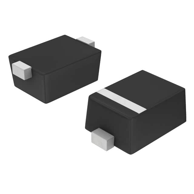
This TVS diode operates within a temperature range of -55°C to 125°C. It is housed in a compact SOD-923 surface mount package, suitable for space-constrained designs. The SZ prefix indicates suitability for automotive applications, with AEC-Q101 qualification and PPAP capability.
Typical applications include USB 2.0 and eSATA interfaces. The device is Pb-Free, Halogen Free/BFR Free, and RoHS Compliant.
| Qty | Low | High |
|---|---|---|
| 1+ | $0.55 | $0.55 |
Estimated market price range - modelled values for guidance only, not live distributor offers.
The working peak voltage (VRWM) is 3.3V from I/O pin to GND.
The breakdown voltage (VBR) at 1mA is 5.5V minimum, 7.0V typical, and 7.8V maximum.
The maximum clamping voltage is 11.2V at the peak pulse current (IPP).
The maximum peak pulse current is 5A for an 8/20µs waveform.
It is available in a surface-mount SOD-923 package.
The maximum capacitance is 0.55pF (I/O to GND), with a typical value of 0.37pF at 1MHz.
It provides ±15kV contact and ±15kV air discharge per IEC 61000-4-2, and ±30kV contact per ISO 10605 (330pF/2kΩ).