

| Distributor | Stock | Pricing | MOQ | PKG | Lead Time | Date Code | On Order Quantity | On Order Delivery | |
|---|---|---|---|---|---|---|---|---|---|
|
76 pcs
|
76 pcs | On Request | 1 | On Request | On Request | 2026-02-25 06:16:38 | On Request | On Request |
| Category | |
| Manufacturer Name | |
| Differential | |
| Frequency | |
| Input | |
| Mounting Type | |
| Number of Circuits | |
| Operating Temperature | |
| Output | |
| Ratio | |
| Supplier Device Package | |
| Tape & Reel | |
| Type | |
| Voltage |
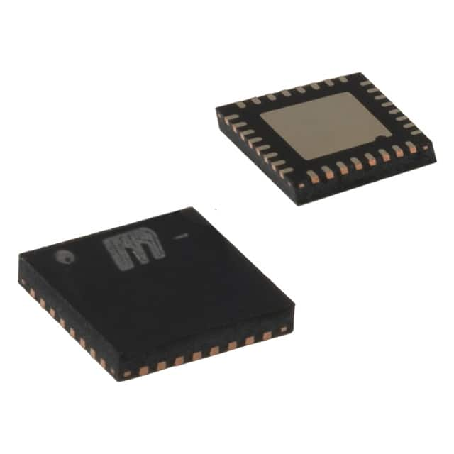
This SY89847UMG from Microchip Technology is a high-performance clock fanout buffer and multiplexer designed for demanding timing applications. It offers a 2:5 input to output ratio, supporting differential inputs and outputs. The device can operate at frequencies up to 2 GHz, making it suitable for high-speed digital systems.
The operating voltage range is from 2.375V to 2.625V, with an operating temperature range of -40°C to 85°C. The SY89847UMG is available in a 32-VFQFN exposed pad package, requiring surface mounting. Its input signal types include CML, LVDS, and PECL, with LVDS output.
This component is ideal for applications requiring precise clock distribution and signal integrity. Its robust design and specifications ensure reliable performance in various electronic systems.
| Qty | Low | High |
|---|---|---|
| 1+ | $4.44 | $4.44 |
Estimated market price range - modelled values for guidance only, not live distributor offers.
The maximum operating frequency for the SY89847UMG is 2 GHz.
The SY89847UMG operates within a supply voltage range of 2.375V to 2.625V.
The SY89847UMG is supplied in a 32-VFQFN exposed pad package.
It supports CML, LVDS, and PECL inputs and LVDS outputs.
The operating temperature range is -40°C to 85°C.