

| Distributor | Stock | Pricing | MOQ | PKG | Lead Time | Date Code | On Order Quantity | On Order Delivery | |
|---|---|---|---|---|---|---|---|---|---|
|
2,070 pcs
|
2070 pcs | On Request | 1 | On Request | On Request | 08+ | On Request | On Request |
| Category | |
| Manufacturer Name | |
| Current | |
| Drain to Source Voltage (Vdss) | |
| Drive Voltage (Max Rds On, Min Rds On) | |
| FET Type | |
| Gate Charge (Qg) (Max) @ Vgs | |
| Input Capacitance (Ciss) (Max) @ Vds | |
| Mounting Type | |
| Operating Temperature | |
| Power Dissipation (Max) | |
| Rds On (Max) @ Id, Vgs | |
| Supplier Device Package | |
| Technology | |
| Vgs (Max) | |
| Vgs(th) (Max) @ Id |
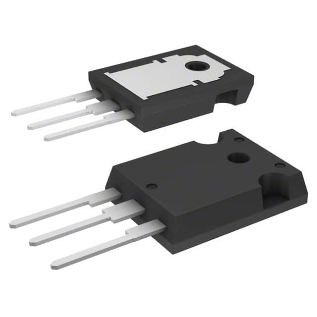
The STMicroelectronics STW19NM65N is an N-Channel MOSFET with a maximum drain-source voltage (Vdss) of 650V and a continuous drain current (Tc) of 15.5A. It features a low on-resistance of 270mOhm at 7.75A and 10V gate-source voltage, with a gate charge (Qg) of 55nC at 10V.
This MOSFET operates at temperatures up to 150°C (TJ) and has a maximum power dissipation of 150W (Tc). It is housed in a TO-247-3 package and is designed for through-hole mounting.
The STW19NM65N utilizes MOSFET (Metal Oxide) technology. Its gate-source voltage (Vgs) maximum is ±25V, and the gate threshold voltage (Vgs(th)) is 4V at 250µA. The drive voltage is 10V for maximum Rds On.
This component is suitable for various power switching applications where high voltage and current handling are required. Its through-hole mounting makes it convenient for traditional PCB designs.
| Qty | Low | High |
|---|---|---|
| 1+ | $2.56 | $2.56 |
Estimated market price range - modelled values for guidance only, not live distributor offers.
The maximum drain-source voltage (Vdss) for the STW19NM65N is 650V.
The continuous drain current (Tc) for the STW19NM65N is 15.5A.
The STW19NM65N comes in a TO-247-3 package.
The maximum operating temperature (TJ) for the STW19NM65N is 150°C.
The RoHS status is RoHS3 Compliant.
The Moisture Sensitivity Level (MSL) is 1 Unlimited.