

| Distributor | Stock | Pricing | MOQ | PKG | Lead Time | Date Code | On Order Quantity | On Order Delivery | |
|---|---|---|---|---|---|---|---|---|---|
|
57 pcs
|
57 pcs | On Request | 1 | On Request | On Request | 09+ | On Request | On Request |
| Category | |
| Manufacturer Name | |
| Drain to Source Voltage (Vdss) | |
| Lead Style | |
| Mounting Type | |
| Package / Case | |
| Power Dissipation | |
| SVHC Present | |
| Tape & Reel |
The STW15N60C3 is an N-channel MOSFET manufactured by Infineon Technologies, designed for robust power applications. It features a high drain-to-source voltage rating of 500V and can handle a continuous drain current of 14.6A at 25°C, with a maximum power dissipation of 190W.
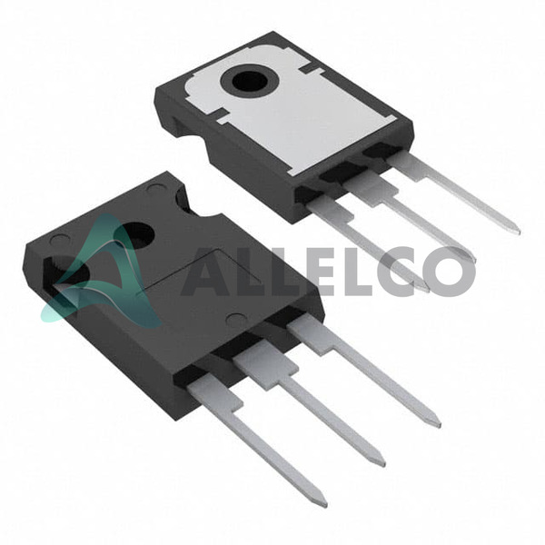
This MOSFET utilizes a TO-247-3 through-hole package, which is suitable for efficient thermal management in high-power scenarios. Key electrical characteristics include a maximum gate-source voltage of ±30V, a gate charge of 80nC at 10V, and input capacitance of 3400pF at 25V. The on-resistance is specified as a maximum of 360mOhm at 7.5A and 10V, indicating low conduction losses.
The threshold voltage is 5V at 250µA. The maximum junction operating temperature is 150°C. This component is suitable for high-voltage, medium-current switching applications where reliable performance and thermal handling are critical.
The maximum drain-source voltage (Vdss) for the STW15N60C3 is 500V.
The continuous drain current (Id) at 25°C is 14.6A.
The maximum power dissipation for the STW15N60C3 is 190W when measured at the case temperature (Tc).
The STW15N60C3 is supplied in a TO-247-3 package.
The STW15N60C3 is mounted using a through-hole method.
The maximum junction operating temperature for the STW15N60C3 is 150°C.