

| Distributor | Stock | Pricing | MOQ | PKG | Lead Time | Date Code | On Order Quantity | On Order Delivery | |
|---|---|---|---|---|---|---|---|---|---|
|
26,567 pcs
|
26567 pcs | On Request | 1 | 25 | On Request | 1123+ | On Request | On Request | |
|
6,866 pcs
|
6866 pcs | On Request | 1 | On Request | On Request | 18+ | On Request | On Request | |
|
1,172 pcs
|
1172 pcs | On Request | 1 | On Request | On Request | 1406 | On Request | On Request |
| Category | |
| Manufacturer Name | |
| Data Rate | |
| Mounting Type | |
| Number of Drivers | |
| Operating Temperature | |
| Operating Voltage | |
| Output Current | |
| Protocol | |
| Storage Temperature | |
| Supplier Device Package | |
| Tape & Reel | |
| Type | |
| Voltage |
The STMicroelectronics STSMIA832TBR is a dual differential line receiver that converts subLVDS clock/datastream signals back into parallel 8-bit CMOS/LVTTL outputs. It is compliant with the Standard Mobile Imaging Architecture (SMIA) specification and supports data rates up to 650 Mbps.
Key electrical characteristics include an operating voltage range of 2.65V to 3.6V and a low power dissipation of 10 µA maximum when disabled. The device features CMOS logic input thresholds and is 3.6V tolerant on specific inputs. It supports SMIA CCP RAW8, RAW10, and RAW12 formats and can be configured for CLASS 0, 1, or 2 modes.
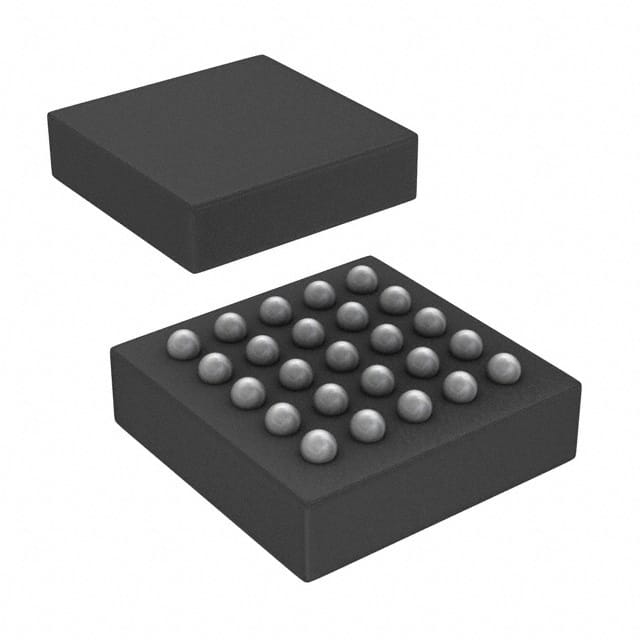
This receiver is housed in a lead-free 25-TFBGA package, optimized for PCB space. It operates within a commercial temperature range of -40°C to 85°C, making it suitable for portable applications. The device is designed to link mobile camera modules to baseband processors, commonly found in feature phones, PDAs, digital cameras, and notebooks.
It supports 32-bit synchronization codes (SOF, EOF, SOL, EOL) to generate H-SYNC and V-SYNC signals. The output LVTTL clock can reach up to 82 MHz, with data outputs strobed on the rising edge.
| Qty | Low | High |
|---|---|---|
| 1+ | $1.44 | $1.44 |
Estimated market price range - modelled values for guidance only, not live distributor offers.
The operating voltage range for the STSMIA832TBR is 2.65 V to 3.6 V for VDD and 1.65 V to 1.95 V for VL.
The STSMIA832TBR supports a maximum input data rate of 650 Mbps.
The STSMIA832TBR operates within a temperature range of -40°C to 85°C.
The STSMIA832TBR is supplied in a 25-TFBGA package.
When disabled (EN = gnd), the STSMIA832TBR has a maximum low power dissipation of 10 µA.