

| Distributor | Stock | Pricing | MOQ | PKG | Lead Time | Date Code | On Order Quantity | On Order Delivery | |
|---|---|---|---|---|---|---|---|---|---|
|
200,000 pcs
|
200000 pcs | On Request | 1 | On Request | On Request | On Request | On Request | On Request |
| Category | |
| Manufacturer Name | |
| Configuration | |
| Current | |
| Drain to Source Voltage (Vdss) | |
| Input Capacitance (Ciss) (Max) @ Vds | |
| Mounting Type | |
| Operating Temperature | |
| Power | |
| Rds On (Max) @ Id, Vgs | |
| Storage Temperature | |
| Supplier Device Package | |
| Technology | |
| Vgs(th) (Max) @ Id |
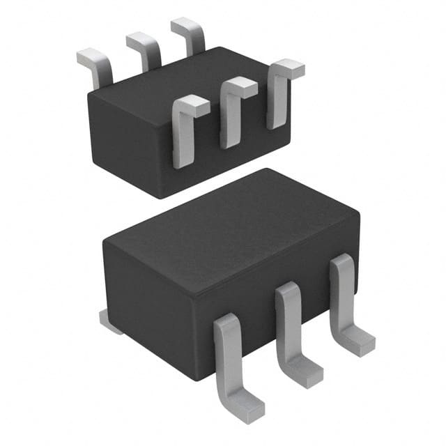
The Toshiba SSM6N16FUTE85LF is a dual N-channel MOSFET (Metal Oxide) designed for low-power switching applications. It integrates two independent N-channel MOSFETs in a single US6 package, offering space-saving benefits for compact designs.
Key electrical specifications include a maximum drain-source voltage of 20V, a continuous drain current of 100mA (200mA pulse), and a maximum drain-source on-resistance of 3Ω at VGS=4V and ID=10mA. The gate threshold voltage is typically 1.1V at 100µA. Input capacitance is 9.3pF at 3V, indicating suitability for high-frequency switching.
The device is housed in a US6 surface-mount package with a maximum power dissipation of 200mW at ambient temperature 25°C. Operating junction temperature range is -55°C to 150°C. This MOSFET array is suitable for load switching, logic level conversion, and signal routing in battery-powered and portable electronics.
| Qty | Low | High |
|---|---|---|
| 1+ | $1.64 | $1.64 |
Estimated market price range - modelled values for guidance only, not live distributor offers.
20V.
100mA.
3Ω maximum at VGS=4V and ID=10mA.
1.1V maximum at VDS=3V and ID=0.1mA.
9.3pF at VDS=3V and f=1MHz.
200mW at Ta=25°C.
Junction temperature up to 150°C, storage temperature -55 to 150°C.