

| Distributor | Stock | Pricing | MOQ | PKG | Lead Time | Date Code | On Order Quantity | On Order Delivery | |
|---|---|---|---|---|---|---|---|---|---|
|
516,571 pcs
|
516571 pcs | On Request | 1 | On Request | On Request | On Request | On Request | On Request |
| Category | |
| Manufacturer Name | |
| Current | |
| Drain to Source Voltage (Vdss) | |
| Drive Voltage (Max Rds On, Min Rds On) | |
| FET Type | |
| Input Capacitance (Ciss) (Max) @ Vds | |
| Lead Style | |
| Mounting Type | |
| Operating Temperature | |
| Power Dissipation (Max) | |
| Rds On (Max) @ Id, Vgs | |
| Storage Temperature | |
| Supplier Device Package | |
| Technology | |
| Turn Off Time | |
| Turn On Time | |
| Vgs (Max) | |
| Vgs(th) (Max) @ Id |
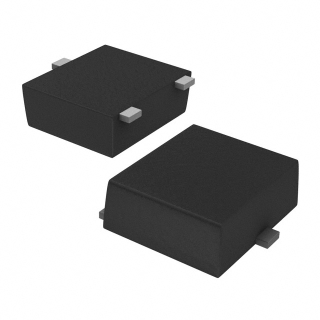
The Toshiba SSM3J117TU,LF is a P-Channel MOSFET suitable for DC-DC converter and high-speed switching applications. It offers a drain-source voltage of 30V and a continuous drain current of 2A at 25°C ambient temperature. The device boasts low ON-resistance, with a maximum of 117 mΩ at 1A and -10V gate-source voltage, and 225 mΩ at 0.5A and -4V gate-source voltage.
This MOSFET is housed in a compact UFM package, designed for surface mounting. It operates at a channel temperature up to 150°C and has a power dissipation of 500mW when mounted on an FR4 board. The P-Channel MOSFET technology ensures efficient power management in various electronic circuits.
Key electrical characteristics include an input capacitance of 280 pF, output capacitance of 80 pF, and reverse transfer capacitance of 45 pF. Switching times are also specified, with a turn-on time of 16 ns and a turn-off time of 35 ns. The gate threshold voltage is a maximum of -2.6V at 1mA, and it supports drive voltages of 4V and 10V.
| Qty | Low | High |
|---|---|---|
| 1+ | $2.56 | $2.56 |
Estimated market price range - modelled values for guidance only, not live distributor offers.
30V.
UFM package with 3-SMD flat leads for surface mount.
The channel temperature maximum is 150°C; storage temperature range is -55°C to 150°C.
2A at Ta=25°C.
117 mΩ at VGS=-10V, ID=-1A.
-1.2V to -2.6V at VDS=-5V, ID=-1mA.
Turn-on time 16ns, turn-off time 35ns.