

| Distributor | Stock | Pricing | MOQ | PKG | Lead Time | Date Code | On Order Quantity | On Order Delivery | |
|---|---|---|---|---|---|---|---|---|---|
|
2,000 pcs
|
2000 pcs | On Request | 1 | On Request | On Request | On Request | On Request | On Request |
| Category | |
| Manufacturer Name | |
| Logic Type | |
| Mounting Type | |
| Number of Bits | |
| Operating Temperature | |
| Supplier Device Package | |
| Supply Voltage |
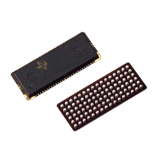
The Texas Instruments SN74SSTU32864CZKER is a versatile 25-bit configurable registered buffer. It supports both 1:1 and 1:2 configurations, allowing for flexibility in system design. This device operates within a supply voltage range of 1.7V to 1.9V and is designed for surface mount installation in a 96-LFBGA package.
Key features include differential clock inputs and SSTL_18 data inputs, with LVCMOS control and reset inputs. The buffer is optimized for DDR2 DIMM PCB layouts and includes output edge-control circuitry to minimize switching noise. It operates across a temperature range of 0°C to 70°C.
This buffer is suitable for applications requiring high-speed data buffering and signal integrity. Its configurable nature and specific pinout optimizations make it ideal for memory module applications and other high-performance digital systems.
| Qty | Low | High |
|---|---|---|
| 1+ | $0.50 | $0.50 |
Estimated market price range - modelled values for guidance only, not live distributor offers.
The supply voltage for the SN74SSTU32864CZKER ranges from 1.7V to 1.9V.
The operating temperature range for the SN74SSTU32864CZKER is 0°C to 70°C.
The SN74SSTU32864CZKER is available in a 96-LFBGA package.
The SN74SSTU32864CZKER is RoHS3 Compliant.
The Moisture Sensitivity Level (MSL) for the SN74SSTU32864CZKER is 1 Unlimited.
The SN74SSTU32864CZKER is REACH Unaffected.