

| Distributor | Stock | Pricing | MOQ | PKG | Lead Time | Date Code | On Order Quantity | On Order Delivery | |
|---|---|---|---|---|---|---|---|---|---|
|
7,232 pcs
|
7232 pcs | On Request | 1 | On Request | On Request | On Request | On Request | On Request | |
|
248 pcs
|
248 pcs | On Request | 1 | On Request | On Request | 15+ | On Request | On Request |
| Category | |
| Manufacturer Name | |
| Input Type | |
| Logic Type | |
| Mounting Type | |
| Number of Bits | |
| Number of Outputs | |
| Operating Temperature Range | |
| Output Type | |
| Supplier Device Package | |
| Supply Voltage |
The SN74SSQEB32882ZALR from Texas Instruments is a JEDEC SSTE32882 compliant 28-bit to 56-bit registered buffer with address-parity test capabilities. This component is designed for operation on DDR3, DDR3L, and DDR3U registered DIMMs, supporting various supply voltages including 1.5V, 1.35V, and 1.25V. It offers 60 CMOS outputs and features a phase-lock loop clock driver for buffering and distributing clock signals.
Key electrical characteristics include a typical additive RMS jitter of 30 fs and compatibility with 1.5V, 1.35V, and 1.25V CMOS inputs. The device supports stacked DDR3 RDIMMs and includes a CKE powerdown mode for optimized system power consumption. The outputs can be driven with configurable strength and skew to enhance signal integrity and compensate for loading.
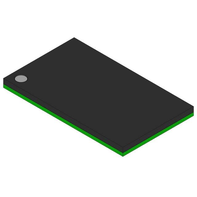
Packaged in a 176-NFBGA (13.5mm x 8mm) with surface mount, the SN74SSQEB32882ZALR operates within a temperature range of 0°C to 85°C. Its design incorporates parity checking on command and address data inputs, making it suitable for applications requiring robust data integrity in high-performance memory modules.
| Qty | Low | High |
|---|---|---|
| 1+ | $4.74 | $4.74 |
Estimated market price range - modelled values for guidance only, not live distributor offers.
The operating temperature range is 0°C to 85°C.
It comes in a 176-NFBGA (13.5x8) surface-mount package.
The typical additive RMS jitter is 30 fs.
It is a 1:2 registered buffer with parity.
It has 60 outputs.