

| Distributor | Stock | Pricing | MOQ | PKG | Lead Time | Date Code | On Order Quantity | On Order Delivery | |
|---|---|---|---|---|---|---|---|---|---|
|
1,589 pcs
|
1589 pcs | On Request | 1 | On Request | On Request | On Request | On Request | On Request |
| Category | |
| Manufacturer Name | |
| Current | |
| Latch-up Performance | |
| Logic Type | |
| Mounting Type | |
| Number of Bits per Element | |
| Number of Channels | |
| Number of Elements | |
| Operating Temperature | |
| Output Type | |
| Propagation Delay | |
| Supplier Device Package | |
| Supplier Package | |
| Supply Current | |
| Voltage |
The SN74LVC541ADWR from Texas Instruments is an octal buffer/driver with 3-state outputs, designed for high-speed digital applications. This component features eight non-inverting buffer channels, controlled by active-low output enable pins.
Key electrical characteristics include an operating voltage range of 1.65V to 3.6V, with inputs capable of accepting voltages up to 5.5V, supporting mixed-mode signal operation. It boasts a very high speed with a maximum propagation delay of 5.1ns at 3.3V. The device provides balanced outputs and supports features like live insertion and partial-power-down mode.
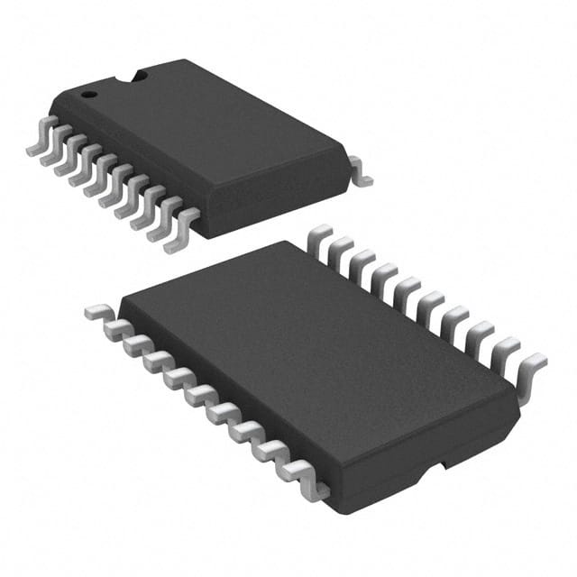
Packaged in a 20-SOIC (0.295", 7.50mm Width) surface-mount form factor, the SN74LVC541ADWR is suitable for various board designs. Its operating temperature range is -40°C to 125°C (TA), making it robust for demanding environments. The latch-up performance exceeds 100mA per JESD 78.
This buffer is ideal for applications requiring signal buffering and level shifting in systems operating at various voltage levels. Its 3-state outputs allow for efficient bus interfacing and power management.
| Qty | Low | High |
|---|---|---|
| 1+ | $0.37 | $0.37 |
Estimated market price range - modelled values for guidance only, not live distributor offers.
The device operates from 1.65V to 3.6V.
It is available in a 20-SOIC package (12.8mm × 10.3mm).
The operating temperature range is -40°C to 125°C.
The device can source or sink 24mA.
Yes, the outputs are 3-state.