

| Distributor | Stock | Pricing | MOQ | PKG | Lead Time | Date Code | On Order Quantity | On Order Delivery | |
|---|---|---|---|---|---|---|---|---|---|
|
72,320 pcs
|
72320 pcs | On Request | 1 | On Request | On Request | On Request | On Request | On Request | |
|
2,581 pcs
|
2581 pcs | On Request | 1 | On Request | On Request | On Request | On Request | On Request | |
|
74 pcs
|
74 pcs | On Request | 1 | On Request | On Request | On Request | On Request | On Request | |
|
25 pcs
|
25 pcs | On Request | 1 | On Request | On Request | On Request | On Request | On Request |
| Category | |
| Manufacturer Name | |
| Applications | |
| Data Rate | |
| Features | |
| Latch-up Performance | |
| Mounting Type | |
| Operating Temperature Range | |
| Propagation Delay | |
| Supplier Device Package | |
| Topology |
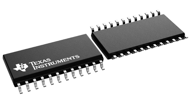
The SN74LVC4245ADW from Texas Instruments is an 8-bit (octal) noninverting bus transceiver designed for translating between 3.3V and 5V environments. It features two separate supply rails, VCCB at 3.3V and VCCA at 5V, enabling bidirectional translation. This device offers a maximum data rate of 200 Mbps and a propagation delay of 6.7 ns.
Key electrical characteristics include an input voltage range of 4.5V to 5.5V and an output voltage range of 2.7V to 5.5V. It provides high drive strength, capable of 24mA at a 3V supply, and features robust, glitch-free power supply sequencing. The transceiver includes VCC isolation and VCC disconnect features, disabling outputs if VCC drops below 100mV or is left floating. Control inputs are referenced to VCCA voltage, and I/O outputs are disabled and become high impedance under specific conditions.
Designed for applications such as GPIO, JTAG, SPI, and UART, the SN74LVC4245ADW operates within a temperature range of -40°C to 85°C. It offers ESD protection exceeding 2000V (Human-Body Model) and 1000V (Charged-Device Model). Latch-up performance is rated above 250mA per JESD 17. The device is available in a 24-SOIC package and supports surface mount.
This transceiver is compatible with the SN74LVC4245A and supports partial-power-down operation via Ioff. Its design ensures reliable performance in mixed-voltage systems.
| Qty | Low | High |
|---|---|---|
| 1+ | $0.80 | $0.80 |
Estimated market price range - modelled values for guidance only, not live distributor offers.
The input voltage range is 4.5 V to 5.5 V, and the output voltage range is 2.7 V to 5.5 V.
The SN74LVC4245ADW is available in a 24-SOIC package.
The operating temperature range is -40°C to 85°C.
The maximum data rate is 200 Mbps.
The propagation delay is 6.7 ns.
ESD protection exceeds 2000V Human-Body Model and 1000V Charged-Device Model per JESD 22.
It is suitable for GPIO, JTAG, SPI, and UART level translation.