

| Distributor | Stock | Pricing | MOQ | PKG | Lead Time | Date Code | On Order Quantity | On Order Delivery | |
|---|---|---|---|---|---|---|---|---|---|
|
1 pcs
|
1 pcs | On Request | 1 | On Request | On Request | On Request | On Request | On Request |
| Category | |
| Manufacturer Name | |
| Current | |
| Latch-up Performance | |
| Logic Type | |
| Mounting Type | |
| Number of Bits per Element | |
| Number of Channels | |
| Number of Elements | |
| Operating Temperature | |
| Output Current | |
| Output Type | |
| SVHC Present | |
| Supplier Device Package | |
| Voltage |
The SN74LVC2G34DCKRG4 from Texas Instruments is a dual, non-inverting buffer gate designed for high-speed operation. It supports a wide supply voltage range from 1.65V to 5.5V, making it versatile for various applications.
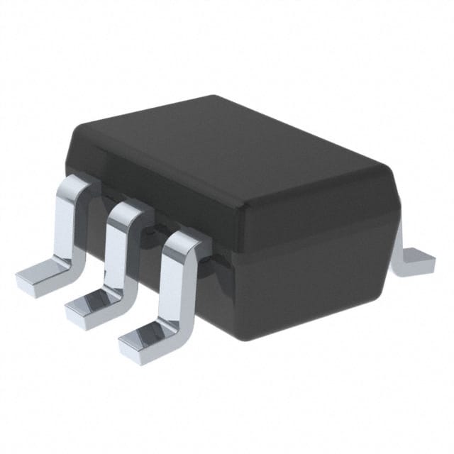
This buffer features a Push-Pull output type and can handle an output current of up to 32mA. The device operates reliably within an ambient temperature range of -40°C to 125°C. It is available in a compact SC-70-6 package, suitable for surface mount applications.
Key electrical characteristics include a maximum propagation delay of 4.1 ns at 3.3V and a low supply current of only 10 µA maximum. The output drive capability is ±24 mA at 3.3V. The component also offers robust ESD protection, exceeding 2000V for the Human Body Model.
This buffer is suitable for applications requiring signal buffering and level shifting where low power consumption and high speed are critical. Its wide voltage range allows interfacing with different logic levels.
| Qty | Low | High |
|---|---|---|
| 1+ | $0.32 | $0.32 |
Estimated market price range - modelled values for guidance only, not live distributor offers.
The operating voltage range is 1.65V to 5.5V.
It is available in an SC-70-6 package.
The operating temperature range is -40°C to 125°C.
It is RoHS3 Compliant.
The MSL is 1 Unlimited.
The maximum propagation delay is 4.1 ns.
The output drive current is ±24 mA.