

| Distributor | Stock | Pricing | MOQ | PKG | Lead Time | Date Code | On Order Quantity | On Order Delivery | |
|---|---|---|---|---|---|---|---|---|---|
|
213,950 pcs
|
213950 pcs | On Request | 1 | On Request | On Request | On Request | On Request | On Request | |
|
123,786 pcs
|
123786 pcs | On Request | 1 | On Request | On Request | On Request | On Request | On Request | |
|
9,024 pcs
|
9024 pcs | On Request | 1 | On Request | On Request | On Request | On Request | 2026-02-16 21:33:16 | |
|
2,500 pcs
|
2500 pcs | On Request | 1 | On Request | On Request | On Request | On Request | On Request |
| Category | |
| Manufacturer Name | |
| Current | |
| Input Logic Level | |
| Logic Type | |
| Max Propagation Delay @ V, Max CL | |
| Mounting Type | |
| Number of Circuits | |
| Number of Inputs | |
| Operating Temperature | |
| Supplier Device Package | |
| Voltage |
The SN74LVC2G04DRLR from Texas Instruments is a dual inverter logic gate. It is designed to operate within a wide voltage range of 1.65V to 5.5V, making it suitable for various applications. This device features a maximum propagation delay of 4.1 ns at 3.3V and provides a significant output drive capability of ±24 mA at 3.3V.
This inverter gate supports partial-power-down applications through its I off circuitry, which prevents damaging current backflow when the device is powered down. The inputs can accept voltages up to 5.5V, offering flexibility in system design. It also boasts low power consumption, drawing a maximum of 10 µA quiescent current.
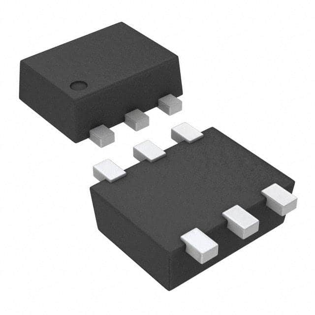
The SN74LVC2G04DRLR is housed in a compact SOT-5X3 package, suitable for surface mount applications. It operates across a temperature range of -40°C to 125°C. The device also includes ESD protection exceeding JESD 22 standards, including the human-body model, machine model, and charged-device model.
Key electrical characteristics include a typical output ground bounce of less than 0.8V and output V OH undershoot greater than 2V at 3.3V and 25°C. Latch-up performance exceeds 100 mA per JESD 78, Class II.
| Qty | Low | High |
|---|---|---|
| 1+ | $0.26 | $0.26 |
Estimated market price range - modelled values for guidance only, not live distributor offers.
The operating voltage range is 1.65V to 5.5V.
The maximum propagation delay is 4.1 ns at 3.3V with 50pF load, and 3.2 ns at 5V with 50pF load.
The operating temperature range is -40°C to 125°C.
The device is available in SOT-5X3, SOT-563, and SOT-666 surface-mount packages.
The maximum quiescent current is 10 µA.
The output drive is ±24 mA at 3.3V.