

| Distributor | Stock | Pricing | MOQ | PKG | Lead Time | Date Code | On Order Quantity | On Order Delivery | |
|---|---|---|---|---|---|---|---|---|---|
|
19 pcs
|
19 pcs | On Request | 1 | On Request | On Request | 04+ | On Request | On Request |
| Category | |
| Manufacturer Name | |
| Data Rate | |
| Features | |
| Input Type | |
| Input Voltage | |
| Latch-up Performance | |
| Mounting Type | |
| Number of Channels | |
| Operating Temperature Range | |
| Output Type | |
| Package / Case |
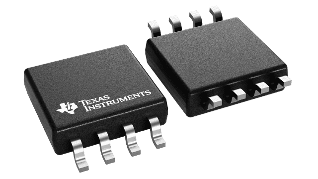
The SN74LVC2G02DCTR is a dual 2-input positive-NOR gate designed for 1.65-V to 5.5-V VCC operation. This device performs the Boolean function Y = A + B or Y = A × B in positive logic.
Key electrical characteristics include a maximum data rate of 100 Mbps, a maximum propagation delay of 4.9 ns at 3.3 V, and an output drive of ±24 mA at 3.3 V. It features over-voltage tolerant inputs, partial power-down (Ioff) support, and very high speed.
The SN74LVC2G02DCTR is available in SSOP, VSSOP, and DSBGA packages. It supports 5-V VCC operation, and its inputs accept voltages up to 5.5 V. The device also offers low power consumption with a maximum ICC of 10 µA.
This logic gate is suitable for various digital applications requiring reliable NOR gate functionality within a wide voltage range. Its features like partial power-down support make it efficient for power-sensitive designs.
The device operates from 1.65 V to 5.5 V.
It is offered in SSOP (DCT), VSSOP (DCU), and DSBGA (YZP) packages, all surface-mount.
The operating temperature range is –40°C to 125°C.
The maximum data rate is 100 Mbps.
Maximum propagation delay is 4.9 ns at 3.3 V.
Output drive is ±24 mA at 3.3 V.