

| Distributor | Stock | Pricing | MOQ | PKG | Lead Time | Date Code | On Order Quantity | On Order Delivery | |
|---|---|---|---|---|---|---|---|---|---|
|
54 pcs
|
54 pcs | On Request | 1 | On Request | On Request | 1436 | On Request | On Request |
| Category | |
| Manufacturer Name | |
| Current | |
| Data Rate (Max) | |
| Input Type | |
| Latch-up Performance | |
| Logic Type | |
| Mounting Type | |
| Number of Channels | |
| Number of Circuits | |
| Number of Inputs | |
| Operating Temperature | |
| Output Type | |
| Schmitt Trigger Input | |
| Supplier Device Package | |
| Voltage |
The Texas Instruments SN74LVC1G0832YZPR is a single 3-input positive AND-OR gate belonging to the LVC technology family. This device performs the Boolean function Y = (A • B ) + C in positive logic. It supports a wide operating voltage range from 1.65V to 5.5V, making it versatile for various applications. The gate features over-voltage tolerant inputs, partial power-down (Ioff) capability, and ultra-high speed operation with a maximum propagation delay of 5 ns at 3.3V. It offers ±24mA output drive at 3.3V and has input hysteresis for improved noise immunity.
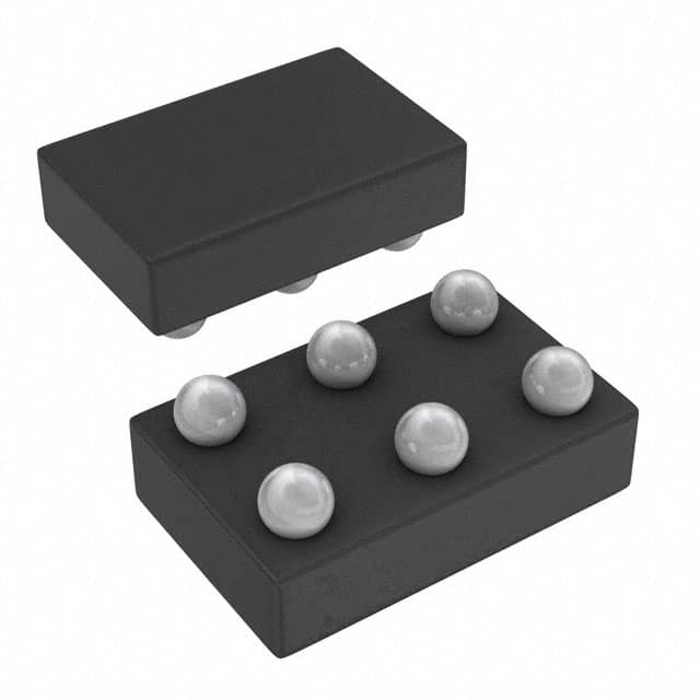
The SN74LVC1G0832YZPR is available in a compact 6-DSBGA package, suitable for space-constrained designs. Its features include support for 5V VCC operation, inputs that accept voltages up to 5.5V, and down translation to VCC. The device also provides low power consumption with a maximum ICC of 10µA. Additional features like live insertion, partial power-down mode, and back-drive protection enhance its usability in complex systems. Latch-up performance exceeds 100mA per JESD 78, Class II, and ESD protection exceeds JESD 22 standards.
This configurable gate can be used in three combinations: as an AND-OR gate, an AND gate, or an OR gate by tying inputs to GND or VCC. Its robust design and versatile functionality make it suitable for a range of digital logic applications where efficient and reliable signal gating is required.
| Qty | Low | High |
|---|---|---|
| 1+ | $0.19 | $0.19 |
Estimated market price range - modelled values for guidance only, not live distributor offers.
1.65V to 5.5V.
6-DSBGA (6-pin DSBGA).
Maximum 5 ns at 3.3V.
±32 mA (sink/source). At 3.3V, typical output drive is ±24 mA.
2000V Human-Body Model, 200V Machine Model, 1000V Charged-Device Model.