

| Distributor | Stock | Pricing | MOQ | PKG | Lead Time | Date Code | On Order Quantity | On Order Delivery | |
|---|---|---|---|---|---|---|---|---|---|
|
405 pcs
|
405 pcs | On Request | 1 | On Request | On Request | On Request | On Request | On Request |
| Category | |
| Manufacturer Name | |
| Current | |
| Data Rate (Max) | |
| Features | |
| Input Type | |
| Latch-up Performance | |
| Lead Spacing | |
| Lead Style | |
| Logic Type | |
| Mounting Type | |
| Number of Channels | |
| Number of Circuits | |
| Number of Inputs | |
| Operating Temperature | |
| Operating Voltage | |
| Output Type | |
| Schmitt Trigger Input | |
| Supplier Device Package | |
| Supplier Package | |
| Voltage |
The SN74LVC1G0832DCKR from Texas Instruments is a single 3-input positive AND-OR gate. It performs the Boolean function Y = (A • B ) + C in positive logic. This device is designed for 1.65-V to 5.5-V VCC operation, accepting input voltages up to 5.5 V and providing down translation to VCC. It offers a maximum propagation delay of 5 ns at 3.3 V and a data rate up to 100 Mbps.
Key features include over-voltage tolerant inputs, partial power-down capability (Ioff), and ultra-high speed. The device consumes low power, with a maximum ICC of 10 µA, and provides ±24-mA output drive at 3.3 V. Input hysteresis allows for slow input transitions and better switching noise immunity. The SN74LVC1G0832DCKR supports live insertion, partial-power-down mode, and back-drive protection. Its latch-up performance exceeds 100 mA per JESD 78, Class II, and ESD protection exceeds JESD 22 standards.
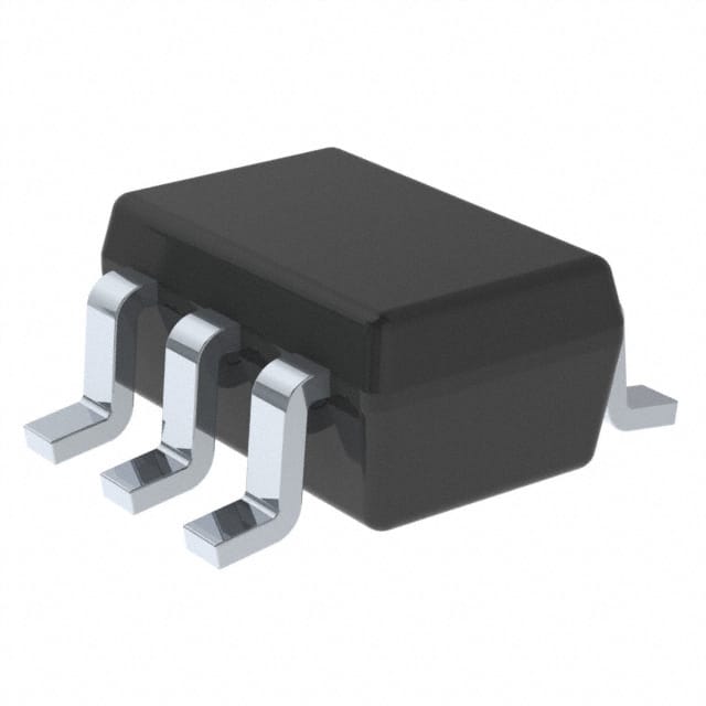
This logic gate is available in the SC-70-6 package, suitable for surface mounting. It can be configured as an AND-OR gate, an AND gate, or an OR gate by tying inputs to GND or VCC. The device is rated for an operating temperature range of -40°C to 125°C.
| Qty | Low | High |
|---|---|---|
| 1+ | $0.26 | $0.26 |
Estimated market price range - modelled values for guidance only, not live distributor offers.
The SN74LVC1G0832DCKR operates from 1.65V to 5.5V.
The maximum data rate for the SN74LVC1G0832DCKR is 100 Mbps.
The SN74LVC1G0832DCKR is available in the SC-70-6 package.
The operating temperature range is -40°C to 125°C.
The output drive is ±24 mA at 3.3 V.