

| Distributor | Stock | Pricing | MOQ | PKG | Lead Time | Date Code | On Order Quantity | On Order Delivery | |
|---|---|---|---|---|---|---|---|---|---|
|
160 pcs
|
160 pcs | On Request | 1 | On Request | On Request | On Request | On Request | On Request |
| Category | |
| Manufacturer Name | |
| Current | |
| Data Rate (Max) | |
| Features | |
| Icc Max | |
| Input Logic Level | |
| Input Type | |
| Latch-up Performance | |
| Logic Type | |
| Max Propagation Delay @ V, Max CL | |
| Mounting Type | |
| Number of Channels | |
| Number of Circuits | |
| Number of Inputs | |
| Operating Temperature | |
| Output Type | |
| SVHC Present | |
| Supplier Device Package | |
| Supplier Package | |
| Voltage |
The SN74LVC1G02DCKTG4 is a single 2-input positive NOR gate designed for 1.65-V to 5.5-V VCC operation. This CMOS device offers high output drive while maintaining low static power dissipation across a broad VCC operating range. It features over-voltage tolerant inputs, partial power-down (Ioff) capability, and ultra-high speed.
The gate performs the Boolean function Y = A + B or Y = A • B in positive logic. Key electrical characteristics include a maximum propagation delay of 4.5ns at 5V and 50pF, a maximum Icc of 10μA, and an output drive of ±24mA at 3.3V. ESD protection exceeds 2000V for the Human-Body Model.
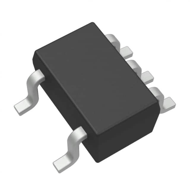
This component is available in the SC-70-5 package, a surface mount type. It is suitable for applications requiring efficient logic operations within a wide voltage range and demanding high-speed performance. The device also supports live insertion and back-drive protection.
| Qty | Low | High |
|---|---|---|
| 1+ | $0.33 | $0.33 |
Estimated market price range - modelled values for guidance only, not live distributor offers.
The SN74LVC1G02DCKTG4 operates from 1.65V to 5.5V.
The maximum propagation delay is 4.5ns at 5V and 50pF.
The SN74LVC1G02DCKTG4 is available in the SC-70-5 package.
The RoHS status is RoHS3 Compliant.
The MSL is 1 Unlimited.