

| Distributor | Stock | Pricing | MOQ | PKG | Lead Time | Date Code | On Order Quantity | On Order Delivery | |
|---|---|---|---|---|---|---|---|---|---|
|
10 pcs
|
10 pcs | On Request | 1 | On Request | On Request | On Request | On Request | On Request |
| Category | |
| Manufacturer Name | |
| Current | |
| Latch-up Performance | |
| Logic Type | |
| Mounting Type | |
| Number of Bits per Element | |
| Number of Channels | |
| Number of Elements | |
| Operating Temperature | |
| Output Type | |
| Supplier Device Package | |
| Supplier Package | |
| Voltage |
The Texas Instruments SN74LVC126APW is a quadruple bus buffer gate designed for 1.65V to 3.6V VCC operation. This device features independent line drivers with 3-state outputs, where each output is disabled when the associated output-enable (OE) input is low.
Key electrical specifications include a supply voltage range of 1.65V to 3.6V and an output current capability of 24mA. The device operates within a temperature range of -40°C to 125°C. It offers very high speed with a maximum propagation delay of 4.7ns at 3.3V. The inputs can accept voltages up to 5.5V, allowing for use in mixed 3.3V and 5V systems.
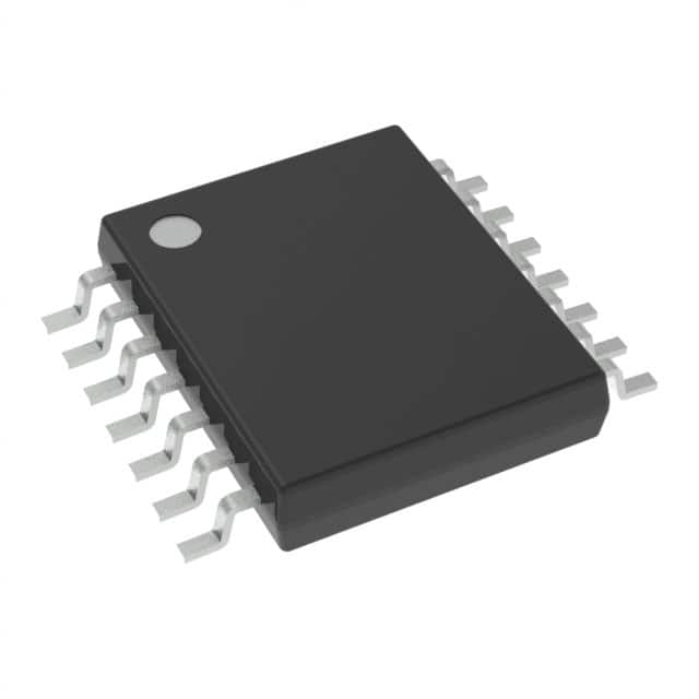
Packaged in a 14-TSSOP, the SN74LVC126APW is suitable for surface mount applications. Its design includes features like balanced outputs and over-voltage tolerant inputs. Latch-up performance exceeds 250mA per JESD 17, and typical output ground bounce is less than 0.8V at 3.3V.
This buffer gate is ideal for applications requiring signal buffering and level translation in mixed-voltage environments. Its 3-state outputs provide flexibility in bus interfacing.
| Qty | Low | High |
|---|---|---|
| 1+ | $0.36 | $0.36 |
Estimated market price range - modelled values for guidance only, not live distributor offers.
The SN74LVC126APW operates from 1.65V to 3.6V.
The SN74LVC126APW is available in a 14-TSSOP package.
The operating temperature range is -40°C to 125°C (TA).
The SN74LVC126APW is RoHS3 Compliant.
The SN74LVC126APW has 4 channels.
The SN74LVC126APW features 3-State outputs.