

| Distributor | Stock | Pricing | MOQ | PKG | Lead Time | Date Code | On Order Quantity | On Order Delivery | |
|---|---|---|---|---|---|---|---|---|---|
|
174 pcs
|
174 pcs | On Request | 1 | On Request | On Request | 1706 | On Request | On Request |
| Category | |
| Manufacturer Name | |
| Current | |
| Industrial Grade | |
| Latch-up Performance | |
| Lead Spacing | |
| Lead Style | |
| Logic Type | |
| Mounting Type | |
| Number of Bits per Element | |
| Number of Channels | |
| Number of Elements | |
| Operating Temperature | |
| Output Type | |
| SVHC Present | |
| Supplier Device Package | |
| Voltage |
The Texas Instruments SN74LVC126ANSR is a quadruple bus buffer gate designed for 1.65V to 3.6V VCC operation. This device features independent line drivers with 3-state outputs, where each output is disabled when the associated output-enable (OE) input is low. It is specified for an operating temperature range of -40°C to 125°C.
Key electrical characteristics include a supply voltage range of 1.65V to 3.6V and an output current capability of 24mA. The device offers very high speed with a maximum propagation delay of 4.7ns at 3.3V. Inputs can accept voltages up to 5.5V, allowing for use in mixed 3.3V and 5V systems. Latch-up performance exceeds 250mA per JESD 17.
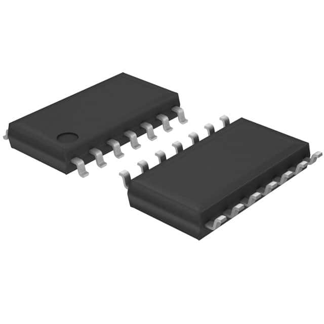
This buffer gate is available in a 14-SOIC surface mount package. The 14-SO (0.209", 5.30mm Width) package is suitable for various electronic designs. To ensure a high-impedance state during power up or power down, the output-enable (OE) must be tied to GND through a pulldown resistor.
The SN74LVC126ANSR is part of the LVC technology family, offering balanced outputs and over-voltage tolerant inputs.
| Qty | Low | High |
|---|---|---|
| 1+ | $0.17 | $0.17 |
Estimated market price range - modelled values for guidance only, not live distributor offers.
The SN74LVC126ANSR operates from 1.65V to 3.6V.
The operating temperature range is -40°C to 125°C.
The SN74LVC126ANSR is available in a 14-SOIC (SO-14) surface-mount package with a 5.30mm body width.
The outputs are 3-state, allowing high-impedance state control via output-enable inputs.
The maximum propagation delay is 4.7ns at 3.3V.
Yes, the inputs accept voltages up to 5.5V.