

| Distributor | Stock | Pricing | MOQ | PKG | Lead Time | Date Code | On Order Quantity | On Order Delivery | |
|---|---|---|---|---|---|---|---|---|---|
|
1,792 pcs
|
1792 pcs | On Request | 1 | On Request | On Request | N/A | On Request | On Request |
| Category | |
| Manufacturer Name | |
| Current | |
| Industrial Grade | |
| Latch-up Performance | |
| Lead Style | |
| Logic Type | |
| Mounting Type | |
| Number of Bits per Element | |
| Number of Elements | |
| Operating Temperature | |
| Output Type | |
| SVHC Present | |
| Supplier Device Package | |
| Voltage |
The Texas Instruments SN74LVC126ADGVR is a quadruple bus buffer gate designed for 1.65V to 3.6V VCC operation. This device features independent line drivers with three-state outputs, where each output is disabled when the associated output-enable (OE) input is low.
Key electrical specifications include an operating voltage range of 1.65V to 3.6V and an operating temperature range of -40°C to 125°C. The inputs can accept voltages up to 5.5V, making it suitable for mixed 3.3V and 5V systems. It offers a maximum propagation delay of 4.7ns at 3.3V and exhibits typical VOLP (output ground bounce) of less than 0.8V and VOHV (output VOH undershoot) of greater than 2V at 3.3V and 25°C.
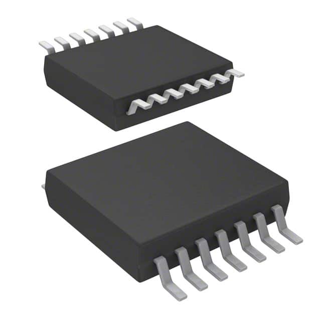
This buffer gate is housed in a 14-TVSOP package, suitable for surface mounting. The standard package quantity is 2000 units on a large tape and reel.
Latch-up performance exceeds 250mA per JESD 17, indicating robust design. The device is specified from -40°C to +125°C, ensuring reliable operation across a wide temperature spectrum.
| Qty | Low | High |
|---|---|---|
| 1+ | $0.14 | $0.14 |
Estimated market price range - modelled values for guidance only, not live distributor offers.
The SN74LVC126ADGVR operates from 1.65V to 3.6V.
The output type is 3-State.
The maximum propagation delay is 4.7ns at 3.3V.
The operating temperature range is -40°C to 125°C.
It is available in a 14-TVSOP (14-TFSOP, 0.173" width) surface mount package.
The logic type is Buffer, Non-Inverting.
Latch-up performance exceeds 250mA per JESD 17.