

| Distributor | Stock | Pricing | MOQ | PKG | Lead Time | Date Code | On Order Quantity | On Order Delivery | |
|---|---|---|---|---|---|---|---|---|---|
|
190 pcs
|
190 pcs | On Request | 1 | On Request | On Request | On Request | On Request | On Request |
| Category | |
| Manufacturer Name | |
| AEC Qualified | |
| Automotive Grade | |
| Current | |
| Industrial Grade | |
| Logic Type | |
| Medical Grade | |
| Military Grade | |
| Mounting Type | |
| Number of Bits per Element | |
| Number of Channels | |
| Number of Elements | |
| Operating Temperature | |
| Output Type | |
| Package / Case | |
| Supplier Device Package | |
| Supplier Package | |
| Voltage | |
| Voltage Supply |
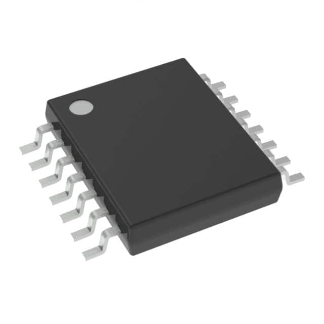
The SN74LVC125A is a quadruple bus buffer gate designed for 1.65V to 3.6V VCC operation. This device features independent line drivers with 3-state outputs, where each output is disabled when its associated output-enable (OE) input is high. The inputs can accept voltages up to 5.5V, allowing for use in mixed 3.3V/5V systems.
Key electrical characteristics include a maximum propagation delay of 4.8ns at 3.3V. The operating temperature range is specified from -40°C to 125°C. The SN74LVC125A is available in a 14-TSSOP package and is suitable for surface mounting.
Applications for this buffer gate include cable modem termination systems, IP phones, optical modules, and various telecommunications infrastructure equipment such as PBXs, TETRA base stations, and telecom shelters. It is also used in vector signal analyzers, video conferencing, and WiMAX equipment.
| Qty | Low | High |
|---|---|---|
| 1+ | $0.38 | $0.38 |
Estimated market price range - modelled values for guidance only, not live distributor offers.
The SN74LVC125APWT operates from 1.65V to 3.6V.
The SN74LVC125APWT is available in a 14-TSSOP package.
The operating temperature range for the SN74LVC125APWT is -40°C to 125°C.
The RoHS Status is listed as RoHS3 Compliant.
The maximum propagation delay is 4.8ns at 3.3V.