

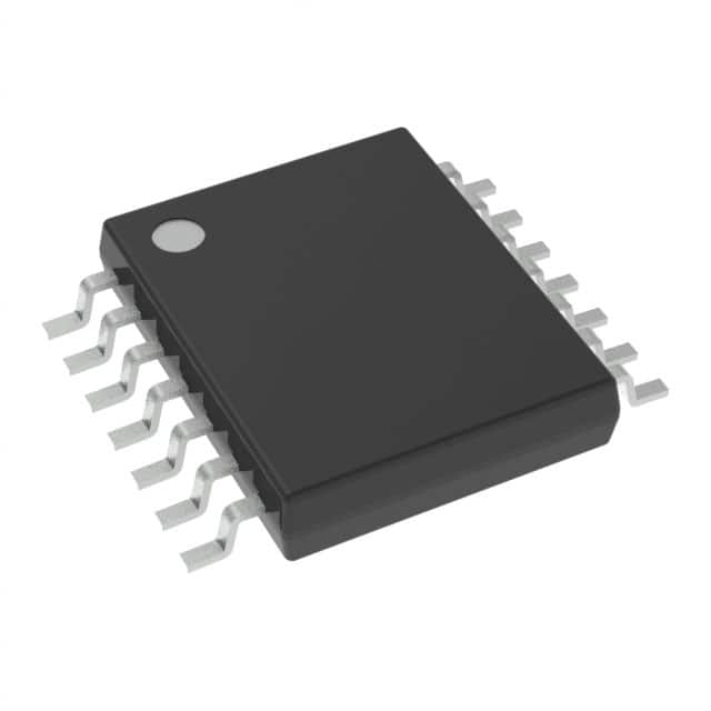
SN74LVC125APWRG4 The SN74LVC125APWRG4 is a quadruple bus buffer gate from Texas Instruments featuring 3-state outputs. It operates from 1.65V to 3.6V and is specified for temperatures between -40°C and 125°C.
Mfr Part #:

SN74LVC125APWRG4

Available from 1 distributors
Mfr Name: Texas Instruments
Texas Instruments
The SN74LVC125APWRG4 is a quadruple bus buffer gate from Texas Instruments featuring 3-state outputs. It operates from 1.65V to 3.6V and is specified for temperatures between -40°C and 125°C.
Total Stock: 376,667 pcs
$ Price Range: $0.22

SN74LVC125APWRG4 Available from 1 distributor

Authorised
Non-Authorised
Distributor Stock Pricing MOQ PKG Lead Time Date Code On Order Quantity On Order Delivery
Non-Authorised Inventory information
376,667 pcs
376667 pcs On Request 1 On Request On Request On Request On Request On Request

SN74LVC125APWRG4 Specifications Quick View

Most important parameters for selection – full specs in datasheet.
Category
Manufacturer Name
Current
Input Voltage
Latch-up Performance
Logic Type
Mounting Type
Number of Bits per Element
Number of Elements
Operating Temperature
Operating Voltage
Output Current
Output Type
Supplier Device Package
Supplier Package
Voltage

SN74LVC125APWRG4 Description

Short technical summary and product information.

The SN74LVC125APWRG4 is a quadruple bus buffer gate designed by Texas Instruments for operation within a 1.65V to 3.6V supply voltage range. This device features independent line drivers with 3-state outputs, where each output is disabled when its associated output-enable (OE) input is high.


Key electrical characteristics include a maximum propagation delay of 4.8ns at 3.3V and an output current capability of ±24mA. The inputs can accept voltages up to 5.5V, allowing for use in mixed 3.3V/5V system environments. The operating temperature range is specified from -40°C to 125°C.


This buffer gate is supplied in a 14-TSSOP package, suitable for surface mounting. The latch-up performance exceeds 250mA per JESD 17, ensuring robust operation.


Applications for this component include cable modem termination systems, IP phones, optical modules, and various wireless infrastructure equipment.

SN74LVC125APWRG4 Quick Information

Product Type: Buffer Gate
Series: SN74LVC125A
Canonical Name: SN74LVC125A Quadruple Bus Buffer Gate with 3-State Outputs
Subcategory: Bus Buffer Gate

SN74LVC125APWRG4 Compliance

RoHS Status: RoHS Compliant
Moisture Sensitivity Level (MSL): 1 Unlimited
REACH Status: REACH Unaffected

SN74LVC125APWRG4 Estimated Pricing

Qty Low High
1+ $0.22 $0.22

Estimated market price range - modelled values for guidance only, not live distributor offers.

SN74LVC125APWRG4 Features

  • Quadruple bus buffer gate with 3-state outputs.
  • Operates from 1.65V to 3.6V supply voltage.
  • Inputs accept voltages up to 5.5V.
  • Specified for -40°C to 125°C operation.
  • Packaged in a 14-TSSOP for surface mounting.

SN74LVC125APWRG4 Applications

  • Suitable for mixed 3.3V/5V systems.
  • Used in telecom and networking equipment.
  • Applicable for optical modules and systems.
  • Supports cable modem termination systems.
  • Ideal for IP phones and wireless infrastructure.

SN74LVC125APWRG4 FAQs

6 frequently asked questions generated from this part’s specifications.
What is the operating voltage range for the SN74LVC125APWRG4?

The operating voltage range for the SN74LVC125APWRG4 is 1.65V to 3.6V.

What is the operating temperature range of the SN74LVC125APWRG4?

The operating temperature range for the SN74LVC125APWRG4 is -40°C to 125°C.

What is the maximum propagation delay of the SN74LVC125APWRG4?

The maximum propagation delay is 4.8ns at VCC = 3.3V.

How many channels does the SN74LVC125APWRG4 have?

The SN74LVC125APWRG4 has 4 channels.

What is the output current capability of this device?

The output current capability is ±24mA.

What is the package type for the SN74LVC125APWRG4?

The package type is 14-TSSOP.

Home
Account

Categories