

| Distributor | Stock | Pricing | MOQ | PKG | Lead Time | Date Code | On Order Quantity | On Order Delivery | |
|---|---|---|---|---|---|---|---|---|---|
|
120 pcs
|
120 pcs | On Request | 1 | On Request | On Request | On Request | On Request | On Request |
| Category | |
| Manufacturer Name | |
| Current | |
| Data Rate | |
| Input Logic Level | |
| Latch-up Performance | |
| Logic Type | |
| Max Propagation Delay @ V, Max CL | |
| Mounting Type | |
| Number of Circuits | |
| Number of Inputs | |
| Operating Temperature | |
| Operating Voltage | |
| Output Current | |
| Supplier Device Package | |
| Supplier Package | |
| Voltage |
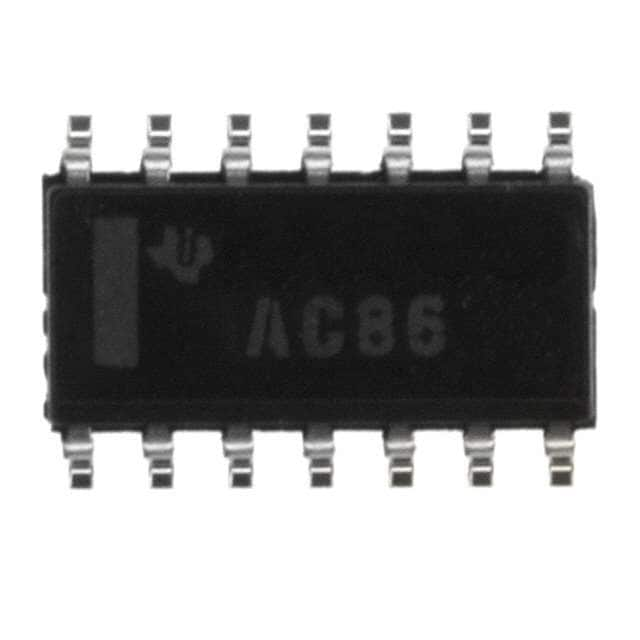
The SN74LVC08ADBR is a quad 2-input AND gate from Texas Instruments, part of the 74LVC family of low-voltage CMOS logic devices. It contains four independent AND gates, each with two inputs, providing the fundamental logic function for digital systems.
This device operates over a wide supply voltage range of 1.65V to 3.6V, making it suitable for low-voltage and battery-powered applications. It features ultra-high-speed operation with a maximum propagation delay of 3.9ns at 3.3V and 50pF load, and supports data rates up to 100 Mbps. The inputs are over-voltage tolerant, and the device supports partial power-down (Ioff) to prevent back-current flow when the supply is off.
The SN74LVC08ADBR is offered in a 14-pin SSOP (Shrink Small Outline Package) with a surface-mount design. It is specified for an extended industrial temperature range of -40°C to 125°C, ensuring reliable operation in harsh environments. ESD protection exceeds 2000V per the Human-Body Model and 1000V per the Charged-Device Model.
| Qty | Low | High |
|---|---|---|
| 1+ | $0.11 | $0.11 |
Estimated market price range - modelled values for guidance only, not live distributor offers.
The operating voltage range is 1.65V to 3.6V.
The operating temperature range is -40°C to 125°C.
The SN74LVC08ADBR comes in a 14-SSOP package.
The maximum propagation delay is 3.9ns at 3.3V and 50pF.
Yes, the SN74LVC08ADBR has over-voltage tolerant inputs.