

| Distributor | Stock | Pricing | MOQ | PKG | Lead Time | Date Code | On Order Quantity | On Order Delivery | |
|---|---|---|---|---|---|---|---|---|---|
|
22 pcs
|
22 pcs | On Request | 1 | On Request | On Request | On Request | On Request | On Request |
| Category | |
| Manufacturer Name | |
| Clock Frequency | |
| Current | |
| Features | |
| Function | |
| Input Capacitance | |
| Input Type | |
| Lead Style | |
| Max Propagation Delay @ V, Max CL | |
| Mounting Type | |
| Number of Bits per Element | |
| Number of Elements | |
| Operating Temperature | |
| Operating Voltage | |
| Output Type | |
| SVHC Present | |
| Supplier Device Package | |
| Supplier Package | |
| Trigger Type | |
| Type | |
| Voltage |
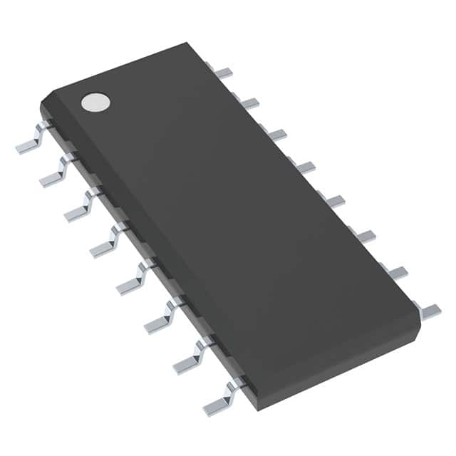
The SN74HC112DR from Texas Instruments is a dual J-K negative-edge-triggered flip-flop IC. It is designed for logic applications requiring precise state control.
This component features two independent J-K flip-flops, each with clear and preset inputs. It supports a clock frequency of up to 24 MHz and operates over a wide voltage range from 2V to 6V. The device exhibits a typical propagation delay of 13ns at 5V and can drive up to 10 LSTTL loads. Its low power consumption is noted at 40µA maximum ICC, with a low input current of 1µA maximum.
The SN74HC112DR is housed in a 16-SOIC package, suitable for surface mount applications. The operating temperature range is specified from -40°C to 85°C.
This versatile flip-flop can function as a toggle flip-flop when J and K inputs are tied high. The negative edge triggering ensures reliable state transitions based on the clock pulse.
| Qty | Low | High |
|---|---|---|
| 1+ | $0.20 | $0.20 |
Estimated market price range - modelled values for guidance only, not live distributor offers.
The operating voltage range is 2V to 6V.
The operating temperature range is -40°C to 85°C.
The SN74HC112DR is available in a 16-SOIC package with a body width of 3.90 mm.
The maximum clock frequency is 24 MHz.
Yes, the outputs are complementary (push-pull).