

| Distributor | Stock | Pricing | MOQ | PKG | Lead Time | Date Code | On Order Quantity | On Order Delivery | |
|---|---|---|---|---|---|---|---|---|---|
|
1,424 pcs
|
1424 pcs | On Request | 1 | On Request | On Request | 10+ | On Request | On Request |
| Category | |
| Manufacturer Name | |
| Circuit | |
| Independent Circuits | |
| Latch-up Performance | |
| Mounting Type | |
| Operating Temperature | |
| Supplier Device Package | |
| Tape & Reel | |
| Type | |
| Voltage | |
| Voltage Supply Source |
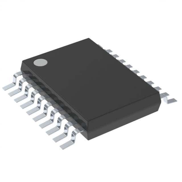
The Texas Instruments SN74CBT3245CDGVR is a high-speed, TTL-compatible FET bus switch designed for various applications including USB interfaces, memory interleaving, and bus isolation. It offers 8 channels in a 1:1 configuration, supporting bidirectional data flow with near-zero propagation delay.
Key electrical characteristics include a low ON-state resistance of 3 Ω typical and low input/output capacitance of 5 pF typical. The device operates within a VCC range of 4V to 5.5V and supports signaling levels from 0V to 5V. It features active undershoot protection up to -2V on the A and B ports, ensuring reliable operation.
This bus switch is supplied in a 20-TVSOP package suitable for surface mounting. It operates across a temperature range of -40°C to 85°C. The SN74CBT3245CDGVR also supports partial-power-down applications with its I off feature, preventing damaging current backflow when the device is powered down.
| Qty | Low | High |
|---|---|---|
| 1+ | $0.29 | $0.29 |
Estimated market price range - modelled values for guidance only, not live distributor offers.
The operating temperature range is -40°C to 85°C.
It is supplied in a 20-TVSOP package.
The typical ON-state resistance is 3 Ω.
The typical input/output capacitance is 5 pF.
The maximum quiescent current consumption is 3 µA.
The ESD performance tested per JESD 22 for the Human-Body Model is 2000 V.
It offers undershoot protection up to -2 V on the A and B ports.