

| Distributor | Stock | Pricing | MOQ | PKG | Lead Time | Date Code | On Order Quantity | On Order Delivery | |
|---|---|---|---|---|---|---|---|---|---|
|
6,000 pcs
|
6000 pcs | On Request | 1 | On Request | On Request | 25+ | On Request | On Request | |
|
2,000 pcs
|
2000 pcs | On Request | 1 | On Request | On Request | On Request | On Request | On Request | |
|
961 pcs
|
961 pcs | On Request | 1 | On Request | On Request | 1340+ | On Request | On Request | |
|
234 pcs
|
234 pcs | On Request | 1 | On Request | On Request | On Request | On Request | On Request |
| Category | |
| Manufacturer Name | |
| AEC Qualified | |
| Automotive Grade | |
| Circuit | |
| Independent Circuits | |
| Industrial Grade | |
| Latch-up Performance | |
| Military Grade | |
| Mounting Type | |
| Operating Temperature | |
| Package Quantity | |
| Supplier Device Package | |
| Type | |
| Voltage | |
| Voltage Supply Source |
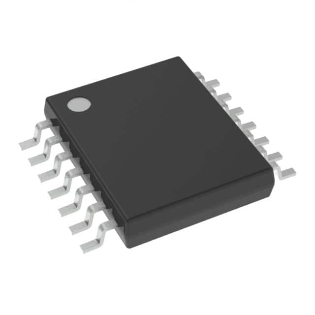
The SN74CB3T3125PWR is a high-speed TTL-compatible FET bus switch manufactured by Texas Instruments. It features 4 independent circuits, each configured as a 1 x 1:1 switch, supporting bidirectional data flow with near-zero propagation delay.
This bus switch operates from a single supply voltage ranging from 2.3V to 3.6V. It offers 5V-tolerant I/Os and supports mixed-mode signal operation, allowing for level shifting from 5V inputs down to 3.3V outputs with a 3.3V VCC, and from 5V/3.3V inputs down to 2.5V outputs with a 2.5V VCC. The device exhibits low ON-state resistance of typically 5 Ω and low input/output capacitance of typically 4.5 pF, minimizing loading effects.
Designed for surface mount, the SN74CB3T3125PWR comes in a 14-TSSOP package. It has a low power consumption with a maximum quiescent current of 20 µA. The device also includes features like undershoot clamp diodes on data and control inputs and supports partial-power-down mode operation. ESD performance is tested per JESD 22 standards, including 2000-V HBM (Class II) and 1000-V CDM.
Key electrical characteristics include a wide range of data I/O signaling levels from 0V to 5V, and control inputs that can be driven by TTL or 5V/3.3V CMOS outputs. Latch-up performance exceeds 250 mA per JESD 17.
| Qty | Low | High |
|---|---|---|
| 1+ | $0.75 | $0.75 |
Estimated market price range - modelled values for guidance only, not live distributor offers.
The operating voltage range is 2.3V to 3.6V.
The device is available in a 14-TSSOP package.
The operating temperature range is -40°C to 85°C.
It has 4 independent circuits.
The typical on-state resistance is 5 ohms.
ESD protection is 2000-V HBM (Class II) and 1000-V CDM.
The maximum quiescent current is 20 µA.