

| Distributor | Stock | Pricing | MOQ | PKG | Lead Time | Date Code | On Order Quantity | On Order Delivery | |
|---|---|---|---|---|---|---|---|---|---|
|
191 pcs
|
191 pcs | On Request | 1 | On Request | On Request | On Request | On Request | On Request |
| Category | |
| Manufacturer Name | |
| Bandwidth | |
| Latch-up Performance | |
| Lead Style | |
| Mounting Type | |
| Operating Temperature | |
| Operating Voltage | |
| Tape & Reel |
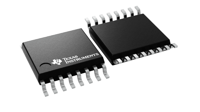
The Texas Instruments SN74CB3Q3253 is a high-bandwidth FET bus switch designed for 2.5-V to 3.3-V operation. It features a data path bandwidth of up to 500 MHz and a low, flat ON-state resistance of typically 4 Ω. This device supports bidirectional data flow with near-zero propagation delay and rail-to-rail switching on data I/O ports.
The SN74CB3Q3253 is suitable for a wide range of signal levels, supporting 0-V to 5-V switching with a 3.3-V VCC and 0-V to 3.3-V switching with a 2.5-V VCC. Its low input/output capacitance minimizes loading and signal distortion. The device operates over a temperature range of -40°C to 85°C and is available in various packages including TVSOP, TSSOP, VQFN, and SSOP.
Key features include 5-V tolerant I/Os, fast switching frequency, and undershoot clamp diodes on data and control inputs. It also supports partial power-down mode operation and exhibits latch-up performance exceeding 100 mA per JESD 78, Class II. ESD protection is provided with 2000-V HBM and 1000-V CDM ratings.
This bus switch is ideal for applications such as USB interfaces, differential signal interface bus isolation, and low-distortion signal gating, supporting both digital and analog signals.
| Qty | Low | High |
|---|---|---|
| 1+ | $0.26 | $0.26 |
Estimated market price range - modelled values for guidance only, not live distributor offers.
The SN74CB3Q3253 has a high-bandwidth data path of up to 500 MHz.
The typical ON-state resistance (ron) is 4 Ω.
The device operates with a VCC range from 2.3 V to 3.6 V.
Data I/Os support 0-V to 5-V signal levels, including 0.8-V, 1.2-V, 1.5-V, 1.8-V, 2.5-V, 3.3-V, and 5-V.
The operating temperature range is -40°C to 85°C.
It is tested per JESD 22 with 2000-V Human-Body Model and 1000-V Charged-Device Model.