

| Distributor | Stock | Pricing | MOQ | PKG | Lead Time | Date Code | On Order Quantity | On Order Delivery | |
|---|---|---|---|---|---|---|---|---|---|
|
2,500 pcs
|
2500 pcs | On Request | 1 | On Request | On Request | On Request | On Request | On Request |
| Category | |
| Manufacturer Name | |
| Clock Frequency | |
| Current | |
| Features | |
| Function | |
| Hysteresis | |
| Input Capacitance | |
| Input Type | |
| Latch-up Performance | |
| Max Propagation Delay @ V, Max CL | |
| Mounting Type | |
| Noise | |
| Number of Bits per Element | |
| Number of Channels | |
| Number of Elements | |
| Operating Temperature | |
| Operating Voltage | |
| Output Type | |
| Supplier Device Package | |
| Supplier Package | |
| Trigger Type | |
| Type | |
| Voltage |
The SN74AUP1G74DQER is a low-power, single positive-edge-triggered D-type flip-flop manufactured by Texas Instruments. It belongs to the AUP technology family and offers a wide operating voltage range from 0.8V to 3.6V, optimized for 3.3V operation.
This flip-flop boasts a maximum clock frequency of 160 MHz and a low supply current of 0.9 µA. Key features include balanced outputs, over-voltage tolerant inputs, partial power-down capability (Ioff), and very high speed with a typical propagation delay of 5 ns at 3.3V. It also incorporates Schmitt-trigger action for improved noise immunity at the input.
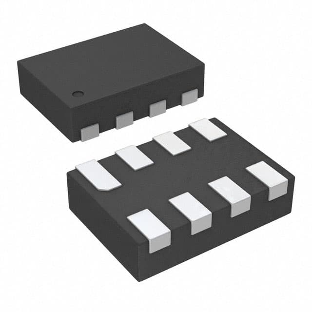
The SN74AUP1G74DQER is available in compact packages such as 8-X2SON, X2SON, VSSOP, DSBGA, and UQFN, suitable for surface mount applications. Its latch-up performance exceeds 100 mA per JESD 78, Class II, and it has undergone ESD performance testing per JESD 22 standards.
Applications for this component include servers, LED displays, network switches, telecom infrastructure, motor drivers, and I/O expanders. Its low power consumption and high-speed capabilities make it suitable for various digital logic designs.
| Qty | Low | High |
|---|---|---|
| 1+ | $0.17 | $0.17 |
Estimated market price range - modelled values for guidance only, not live distributor offers.
The operating voltage range is 0.8V to 3.6V.
The primary package is 8-X2SON (1.4x1 mm). Additional packages include DSBGA, X2SON (DQE), VSSOP, DSBGA (YFP), and UQFN.
The operating temperature range is -40°C to 85°C.
The maximum clock frequency is 160 MHz.
The maximum propagation delay is 5 ns at 3.3V.
Yes, inputs are tolerant up to 3.6V.
ESD performance is 2000-V Human-Body Model (A114-B, Class II) and 1000-V Charged-Device Model (C101).