

| Distributor | Stock | Pricing | MOQ | PKG | Lead Time | Date Code | On Order Quantity | On Order Delivery | |
|---|---|---|---|---|---|---|---|---|---|
|
177 pcs
|
177 pcs | On Request | 1 | On Request | On Request | On Request | On Request | On Request |
| Category | |
| Manufacturer Name | |
| AEC Qualified | |
| Automotive Grade | |
| Current | |
| Industrial Grade | |
| Latch-up Performance | |
| Logic Type | |
| Medical Grade | |
| Military Grade | |
| Mounting Type | |
| Number of Bits per Element | |
| Number of Elements | |
| Operating Temperature | |
| Output Type | |
| Propagation Delay | |
| Supplier Device Package | |
| Supplier Package | |
| Supply Current | |
| Voltage |
The SN74AUC16244DGVR from Texas Instruments is a 16-bit buffer/driver designed for high-performance applications. It is part of the Widebus family and is optimized for 1.8-V operation while supporting 3.6-V I/O tolerant mixed-mode signal operation.
This device provides true outputs and symmetrical active-low output-enable (OE) inputs. It can be configured as four 4-bit buffers, two 8-bit buffers, or one 16-bit buffer, offering flexibility in design. The buffer/driver operates from 0.8V to 2.7V, with specific design focus on 1.65V to 1.95V VCC operation. Key electrical characteristics include a maximum propagation delay of 2ns at 1.8V and ±8mA output drive at 1.8V. It also features low power consumption with a maximum ICC of 20µA.
The SN74AUC16244DGVR is specified for partial-power-down applications using Ioff, which disables outputs to prevent damaging current backflow when the device is powered down. ESD protection exceeds JESD 22 standards, including 2000V for the Human-Body Model, 200V for the Machine Model, and 1000V for the Charged-Device Model. Latch-up performance exceeds 100mA per JESD 78, Class II.
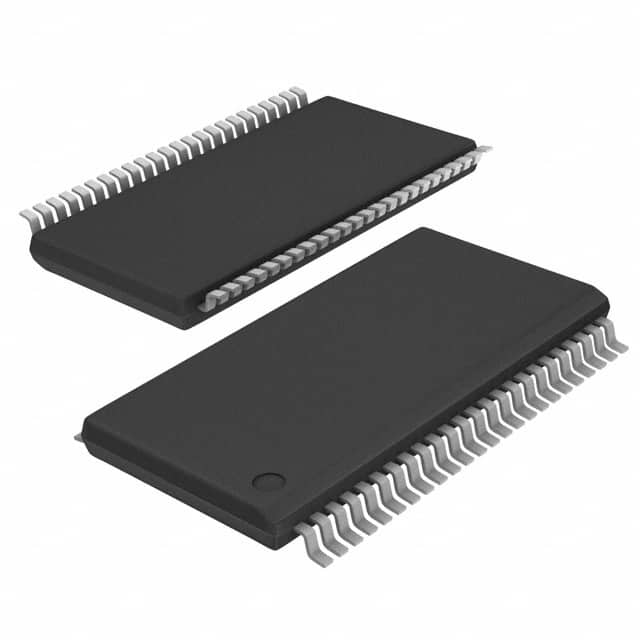
Packaged in a 48-TVSOP, this surface-mount device is suitable for various bus-oriented applications, including memory address drivers and clock drivers. The operating temperature range is -40°C to 85°C.
| Qty | Low | High |
|---|---|---|
| 1+ | $1.20 | $1.20 |
Estimated market price range - modelled values for guidance only, not live distributor offers.
The supply voltage range is 0.8V to 2.7V, designed for operation with a VCC of 1.65V to 1.95V.
The output drive current is ±8mA at 1.8V.
The maximum propagation delay is 2ns at 1.8V.
The maximum supply current is 20µA.
The operating temperature range is -40°C to 85°C.
ESD protection is rated at 2000V for the human-body model, 200V for the machine model, and 1000V for the charged-device model.
The device is available in 48-TVSOP and 48-TFSOP surface-mount packages.