

| Distributor | Stock | Pricing | MOQ | PKG | Lead Time | Date Code | On Order Quantity | On Order Delivery | |
|---|---|---|---|---|---|---|---|---|---|
|
3,147 pcs
|
3147 pcs | On Request | 1 | On Request | On Request | On Request | On Request | On Request | |
|
1 pcs
|
1 pcs | On Request | 1 | On Request | On Request | 18+ | On Request | On Request |
| Category | |
| Manufacturer Name | |
| Current | |
| Latch-up Performance | |
| Lead Spacing | |
| Logic Type | |
| Mounting Type | |
| Number of Bits per Element | |
| Number of Elements | |
| Operating Temperature | |
| Output Type | |
| Propagation Delay | |
| Storage Temperature | |
| Supplier Device Package | |
| Tape & Reel | |
| Voltage |
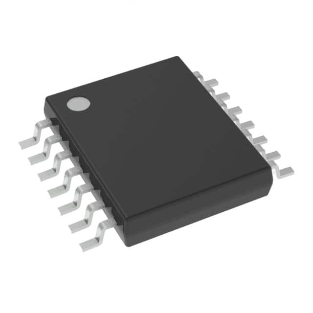
The SN74ALVC125PWR is a quadruple bus buffer gate manufactured by Texas Instruments, designed for 1.65V to 3.6V VCC operation. This device features independent line drivers with 3-state outputs, where each output is disabled when its associated output-enable (OE) input is high. It offers a maximum propagation delay of 2.8ns at 3.3V and ±24mA output drive at 3.3V. The latch-up performance exceeds 250mA per JESD 17, and ESD performance exceeds 2000V (Human-Body Model), 200V (Machine Model), and 1000V (Charged-Device Model).
This buffer gate is suitable for various digital applications requiring signal buffering and isolation. It is available in a 14-TSSOP package, designed for surface mounting. The operating temperature range is -40°C to 85°C (TA). To ensure a high-impedance state during power-up or power-down, the OE input should be tied to VCC through a pullup resistor.
| Qty | Low | High |
|---|---|---|
| 1+ | $0.39 | $0.39 |
Estimated market price range - modelled values for guidance only, not live distributor offers.
The SN74ALVC125PWR operates from 1.65V to 3.6V.
The SN74ALVC125PWR is available in a 14-TSSOP package.
The operating temperature range is -40°C to 85°C.
The SN74ALVC125PWR is RoHS3 Compliant.