

| Distributor | Stock | Pricing | MOQ | PKG | Lead Time | Date Code | On Order Quantity | On Order Delivery | |
|---|---|---|---|---|---|---|---|---|---|
|
361,600 pcs
|
361600 pcs | On Request | 1 | On Request | On Request | On Request | On Request | On Request | |
|
2,524 pcs
|
2524 pcs | On Request | 1 | On Request | On Request | On Request | On Request | On Request | |
|
1 pcs
|
1 pcs | On Request | 1 | On Request | On Request | On Request | On Request | On Request | |
|
1 pcs
|
1 pcs | On Request | 1 | On Request | On Request | On Request | On Request | On Request |
| Category | |
| Manufacturer Name | |
| Current | |
| Failure Rate | |
| Input Logic Level | |
| Latch-up Performance | |
| Lead Spacing | |
| Lead Style | |
| Logic Type | |
| Max Propagation Delay @ V, Max CL | |
| Mounting Type | |
| Number of Circuits | |
| Number of Inputs | |
| Operating Temperature | |
| Quiescent Current | |
| Supplier Device Package | |
| Tape & Reel | |
| Voltage |
The SN74ALVC08DR is a quadruple 2-input positive-AND gate from Texas Instruments, operating from a 1.65V to 3.6V supply voltage. This device performs the Boolean function Y = A · B.
Key electrical characteristics include a maximum propagation delay of 2.9ns at 3.3V with a 50pF load capacitance. The output drive capability is ±24mA at 3.3V. It also features ESD protection exceeding JESD 22 standards and latch-up performance exceeding 250mA per JESD 17.
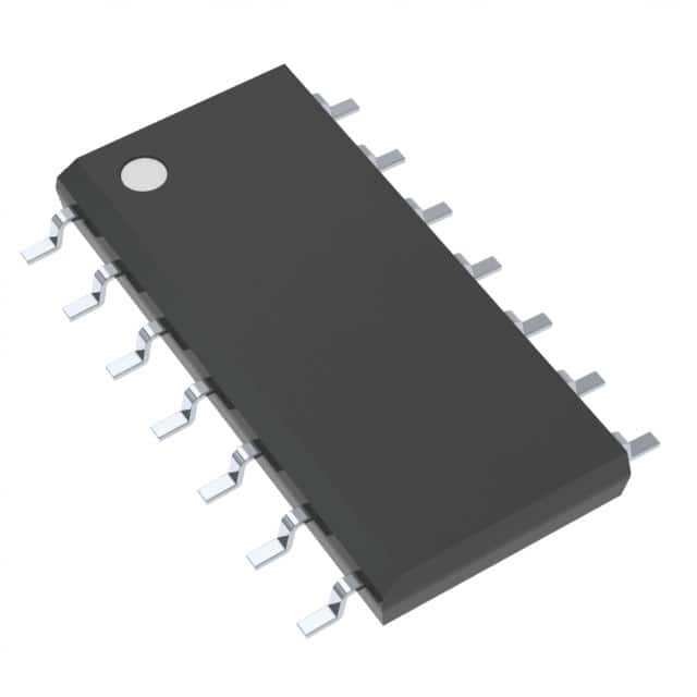
This component is housed in a 14-SOIC surface-mount package. The operating temperature range is -40°C to 85°C. Its design is suitable for applications requiring reliable AND logic functions within the specified voltage and temperature ranges.
| Qty | Low | High |
|---|---|---|
| 1+ | $0.22 | $0.22 |
Estimated market price range - modelled values for guidance only, not live distributor offers.
The SN74ALVC08DR operates from 1.65V to 3.6V.
The maximum propagation delay is 2.9ns at 3.3V and 50pF load.
The operating temperature range is -40°C to 85°C.
The SN74ALVC08DR is available in a 14-SOIC package (0.154", 3.90mm Width).
The output drive current is ±24mA.
The maximum quiescent current is 10µA.
The device has ESD protection of 2000V HBM, 200V MM, and 1000V CDM.