

| Distributor | Stock | Pricing | MOQ | PKG | Lead Time | Date Code | On Order Quantity | On Order Delivery | |
|---|---|---|---|---|---|---|---|---|---|
|
200,000 pcs
|
200000 pcs | On Request | 1 | On Request | On Request | On Request | On Request | On Request |
| Category | |
| Manufacturer Name | |
| Current | |
| Input Logic Level | |
| Logic Type | |
| Max Propagation Delay @ V, Max CL | |
| Mounting Type | |
| Number of Circuits | |
| Number of Inputs | |
| Operating Temperature | |
| Supplier Device Package | |
| Voltage |
The SN74ALVC00DGVR is a quadruple 2-input positive-NAND gate designed for operation from 1.65V to 3.6V VCC. This device performs the Boolean function Y = (A ⋅ B) or Y = A + B in positive logic.
Key electrical characteristics include an operating voltage range of 1.65V to 3.6V, a maximum propagation delay of 3ns at 3.3V with a 50pF load, and an output drive of ±24mA at 3.3V. The input logic levels range from 1.7V to 2V.
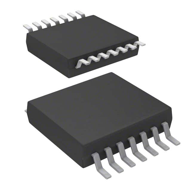
This NAND gate is housed in a 14-TVSOP package and features a surface mount type. The operating temperature range is -40°C to 85°C. Latch-up performance exceeds 250mA per JESD 17, and ESD protection exceeds JESD 22 standards.
This component is suitable for various digital logic applications requiring high-speed NAND gate functionality within the specified voltage and temperature ranges.
| Qty | Low | High |
|---|---|---|
| 1+ | $0.14 | $0.14 |
Estimated market price range - modelled values for guidance only, not live distributor offers.
The supply voltage range is 1.65V to 3.6V.
It contains 4 NAND gates, each with 2 inputs.
The output current is 24mA for both high and low outputs.
The maximum propagation delay is 3ns at 3.3V with a 50pF load.
The operating temperature range is -40°C to 85°C.
It is available in a 14-TVSOP surface mount package (14-TFSOP, 0.173" width, 4.40mm width).
The input logic level range is 1.7V to 2V.