

| Distributor | Stock | Pricing | MOQ | PKG | Lead Time | Date Code | On Order Quantity | On Order Delivery | |
|---|---|---|---|---|---|---|---|---|---|
|
128 pcs
|
128 pcs | On Request | 1 | On Request | On Request | 07+ | On Request | On Request |
| Category | |
| Manufacturer Name | |
| Input Type | |
| Lead Style | |
| Number of Channels | |
| Operating Temperature Range | |
| Output Type | |
| Package / Case | |
| Tape & Reel |
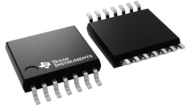
The SN74AHCT125PWR is a quadruple bus buffer gate manufactured by Texas Instruments. It belongs to the AHCT technology family and features independent line drivers with 3-state outputs. Each output is disabled when its associated output-enable (OE) input is high. When OE is low, the gate passes data from the A input to its Y output.
Key electrical specifications include a nominal supply voltage of 5V, with a range of 4.5V to 5.5V. The device supports TTL-compatible CMOS inputs and 3-state outputs. It offers a maximum output current (IOL) of 8mA and a maximum output current (IOH) of -8mA. The maximum supply current is 20µA. The operating temperature range is from -40°C to 125°C, and it exhibits very high speed with propagation delays typically between 5-10ns.
This component is suitable for various digital logic applications requiring buffering and signal isolation. Its 3-state output capability allows it to be connected to a common bus without interfering with other devices when disabled. The device is available in multiple package types, including SOP, TSSOP, WQFN, TVSOP, PDIP, SOIC, SSOP, and VQFN.
Design considerations include ensuring proper handling of the output-enable signal for high-impedance state during power up or power down, potentially requiring a pullup resistor to VCC. The latch-up performance exceeds 250mA per JESD 17, and the inputs are over-voltage tolerant.
The device operates from 4.5V to 5.5V, with a nominal supply voltage of 5V.
The SN74AHCT125PWR is supplied in a TSSOP (PW) package.
It operates from -40°C to 125°C.
It has 4 independent buffer channels.
The outputs are 3-state, allowing high-impedance, high, or low states.
The maximum supply current is 20 µA.
The propagation delay is 5 to 10 nanoseconds.