

| Distributor | Stock | Pricing | MOQ | PKG | Lead Time | Date Code | On Order Quantity | On Order Delivery | |
|---|---|---|---|---|---|---|---|---|---|
|
1,077 pcs
|
1077 pcs | On Request | 1 | On Request | On Request | On Request | On Request | On Request |
| Category | |
| Manufacturer Name | |
| ESD Protection | |
| Mounting Type | |
| Number of Drivers | |
| Operating Temperature | |
| Protocol | |
| Supplier Device Package | |
| Type | |
| Voltage |
The SN65LVDS822RGZR from Texas Instruments is an advanced FlatLink low-voltage differential signal (LVDS) receiver. It is built on a modern CMOS process and offers several key features for efficient data deserialization. The device supports deserialization modes of 4:27 and 2:27, with a pixel clock range from 4 MHz to 54 MHz, suitable for resolutions from 160x120 up to 1024x600.
This LVDS receiver operates with a single 3.3V power supply, and its VDDIO can be set from 1.8V to 3.3V for flexible panel support. It includes selectable CMOS output slew rates for reduced EMI, integrated switchable input termination, and failsafe input pins with ±3 kV HBM ESD protection. The device is compatible with TIA/EIA-644-A transmitters and TI FlatLink transmitters like the SN75LVDS83B and SN65LVDS93A.
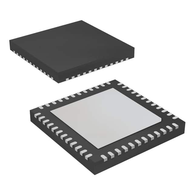
The SN65LVDS822RGZR is packaged in a 48-pin VQFN (7x7 mm) with an exposed pad, designed for surface mounting. It features automatic low-power Standby and Shutdown modes to conserve energy when the LVDS clock is disabled or a low voltage is applied to the SHTDN# pin. The operating temperature range is -40°C to 85°C.
| Qty | Low | High |
|---|---|---|
| 1+ | $3.13 | $3.13 |
Estimated market price range - modelled values for guidance only, not live distributor offers.
The operating temperature range is -40°C to 85°C.
The SN65LVDS822RGZR is available in a 48-VQFN (7x7) package and a 48-VFQFN Exposed Pad package.
The pixel clock range is from 4 MHz to 54 MHz.
It supports 4:27 and 2:27 deserialization modes.
It has ±3 kV HBM ESD protection.