

| Distributor | Stock | Pricing | MOQ | PKG | Lead Time | Date Code | On Order Quantity | On Order Delivery | |
|---|---|---|---|---|---|---|---|---|---|
|
94 pcs
|
94 pcs | On Request | 1 | On Request | On Request | On Request | On Request | On Request | |
|
37 pcs
|
37 pcs | On Request | 1 | On Request | On Request | On Request | On Request | On Request |
| Category | |
| Manufacturer Name | |
| AEC Qualified | |
| Automotive Grade | |
| Capacitance | |
| Clock Frequency | |
| Current | |
| Data Rate (Max) | |
| Delay Time | |
| Industrial Grade | |
| Input | |
| Medical Grade | |
| Military Grade | |
| Mounting Type | |
| Number of Channels | |
| Operating Temperature | |
| Output | |
| Supplier Device Package | |
| Type | |
| Voltage |
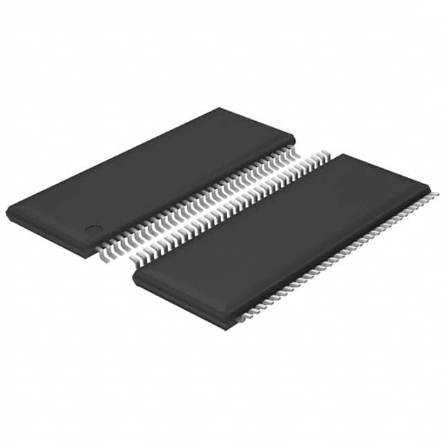
The SN65LVDS117DGG from Texas Instruments is a dual 8-port LVDS repeater, functioning as a buffer and multiplexer. It is engineered to meet or exceed the requirements of the ANSI EIA/TIA-644 standard for controlled impedance media.
This device supports typical data signaling rates up to 400 Mbps and clock frequencies up to 400 MHz. It operates within a voltage range of 3V to 3.6V and features a low-voltage differential signaling (LVDS) interface. Key electrical characteristics include a propagation delay of 2.8ns, output skew less than 550 ps, bank skew less than 150 ps, and part-to-part skew less than 1.5 ns.
The SN65LVDS117DGG is housed in a 64-TSSOP package and is designed for surface mounting. Its operating temperature range is -40°C to 85°C. The repeater includes enabling logic for individual control of output pairs and all outputs, making it suitable for complex clock and data distribution systems.
| Qty | Low | High |
|---|---|---|
| 1+ | $7.26 | $7.26 |
Estimated market price range - modelled values for guidance only, not live distributor offers.
The maximum data signaling rate is 400 Mbps.
The operating temperature range is -40°C to 85°C.
It is supplied in a 64-TSSOP package.
The typical output voltage is 350 mV.
The propagation delay time is 2.8ns.